

Neuromorphic Computing
Neuromorphic CMOS-MoS2 Based Hybrid System for Low Power Edge-Computing
Team Members: Pratik Kumar, Sarthak Gupta
The next generation computational architectures require embedding deep learning, machine learning and artificial intelligence onto computationally efficient hardware and devices with low energy footprints. This is necessitated by an ever-increasing demand in computing power, which, coupled with data explosion is pushing the boundaries of conventional computational architectures. We have proposed one such hybrid architecture based on neuromorphic population coding, where encoding of information is carried out by the activity in an ensemble of neurons such as in the olfactory, motor, and visual cortex. Our proposed hybrid architecture utilizes a CMOS-based silicon neuron as a basic computing element, and molybdenum disulphide (MoS2) based two-dimensional synaptic memtransistor as an analogue memory, instead of conventional digital memories, to avoid bottleneck in terms of power and area. A combination of silicon technology with 2D materials can surpass the current technology limitation and can offer remarkable advancements in circuit architecture and device performance at atomic levels.
In this regard, the propose a biologically inspired wake-up system, shown in Fig 1, with embedded intelligence and energy efficient footprint, that can be integrated with existing edge computing devices to improve their energy and performance. This system exploits the inherent mismatches present in lower silicon technology nodes to reduce computational complexity and simultaneously uses multi-state memtransistive device for low power computation and reduced computational complexity. In the current hybrid framework, this synaptic memtransistor memory provides two functions simultaneously, one a substitute for digital memories as an adaptable multi-state memductance and the other is the execution of an inherent multiplication operation by Kirchhoff’s current law (KCL), thus offering a low power computational paradigm. From the promising results for demonstrated regression and classification tasks, this framework proves to be a step closer for designing a low power, reduced dimensions, fault-tolerant, and robust architecture. These characteristics enable the framework to be employed in onsite processing of data such as in IOT devices, edge devices, energy- and area-constrained devices or devices with low computational resources.
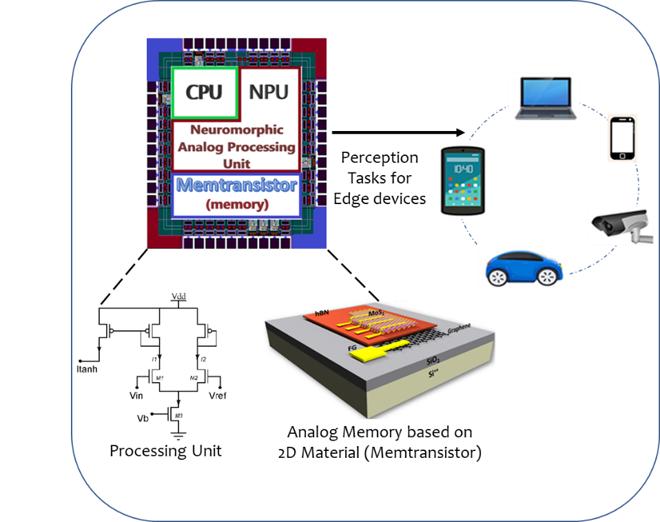
Fig. 1 | Chip architecture with functional blocks and applications
-
-
-
Gupta S, Kumar P, Paul T, van Schaik A, Ghosh A, Thakur C S, (2019) “Low Power, CMOS-MoS2 Memtransistor based Neuromorphic Hybrid Architecture for Wake-Up Systems“. Scientific Reports (Nature Group)
-
-
Fully Programmable Neuromorphic Chip Architecture
Team Members: Pratik Kumar, Pallab Kumar Nath, Satyam Shivam, Nazreen PM
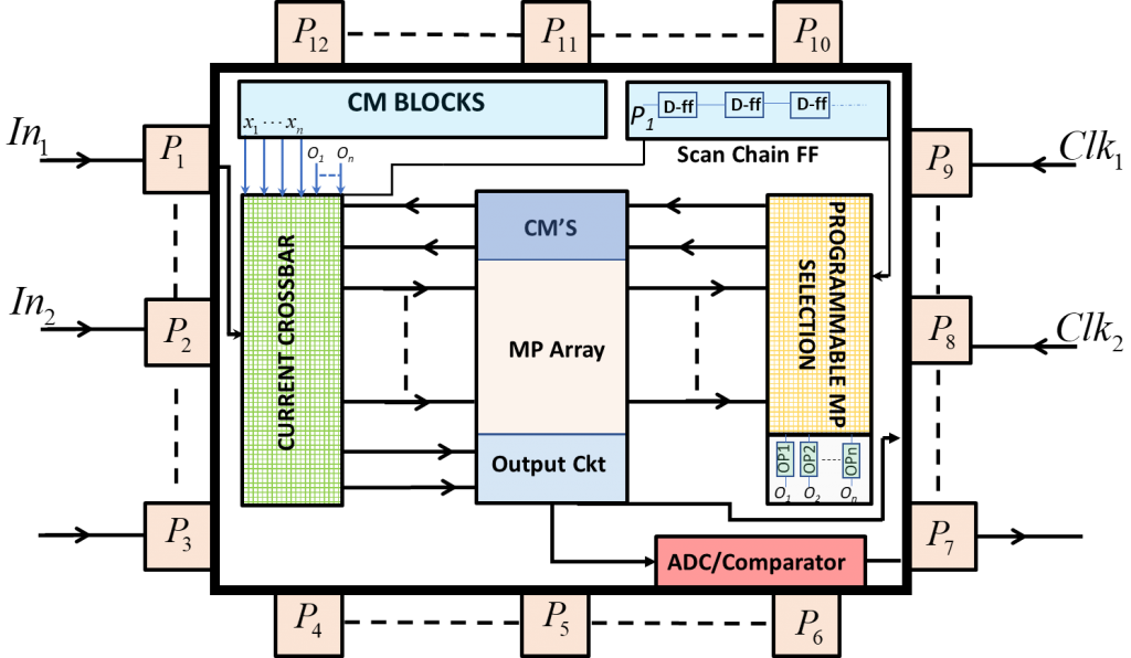
Fig. 2 | Top Level Chip Architectural Block
The next era of computing for artificial intelligence (AI) requires efficient hardware with increased computational performances and ultra-low energy footprint. This requires a disruptive approach in architecture design, unlike the traditional von Neumann approach which is serial in nature. Presently, the computations are achieved by CPUs, GPUs and TPUs which utilises von Neumann architectures to perform multiply and accumulate (MAC) operations in parallel. Such architectures have large energy and memory footprints. In contrast, the neuromorphic architectures are inspired by neurobiological systems and have characteristics such as in-memory computing, stochastic computing and massive network fan-outs. They are parallel and distributed architectures which exhibit low precision along with adaptive learning. A significant improvement in energy and other performance footprints can be obtained by implementing such architectures in analogue. But the analogue implementation of such architectures comes with its own challenges such as the designed hardware is sensitive to device mismatch and other non-linear effects. Furthermore, the designed architecture depends on the physical responses of the MOS transistors operating in different biasing regimes and hence requires distinct circuit architecture for different computational operations. These challenges along with other trade-offs limit the flexibility in design parameters and put performance and power restrictions on the designed circuit. The proposed hardware software-based co-design platform can achieve a significant boost in performance, power and accuracy. We are working on designing the bias scalable neuromorphic architecture that is invariant to design parameters and operating regimes.
-
-
-
S.Gupta, P. Kumar, K. Kumar, S. Chakraborty, Thakur, C. S, “Low Power Neuromorphic Analog System based on Sub-Threshold Current Mode Circuits“.IEEE International Symposium on Circuits and Systems (ISCAS), 2019.\
-
Nazreen P.M., S. Chakrabartty S., Thakur C.S. “Multiplierless and Sparse Machine Learning based on Margin Propagation Networks“. arXiv:1910.
-
-
Neuromorphic In-Memory Computing Framework for Low-Power Computational tasks
Team Members: Pratik Kumar, Abhishek Ramdas Nair
Due to the proliferation of internet-of-things (IoTs) in the areas of ubiquitous sensing and human-machine interaction, there has been an increased demand towards integrating intelligence directly onto IoT hardware platforms. In these embedded platforms, high energy-efficiency and low computational/ memory foot-print are the key design requirements due to limited battery resources. In this regard, wake-up systems play an integral role and operate by triggering on the computationally and power-intensive modules only when some ambient conditions are detected. Memtransistor crossbar arrays have shown great potential for neuromorphic computing and learning. These non-volatile memories if arranged in crossbar pattern as shown in Fig.3(d) can carry out array size in-memory MVM and addition using Kirchhoff’s current law (KCL) in a single time step. Each column of memtransistor crossbar array represents single template vector with rows equal to the number of features stored as memductance (conductance of memtransistor device). Fig.4 shows a generic memtransistors based classification framework. Energy consumption in fabricated memtransistor was found to be 0.7nJ for potentiation and 0.5 pJ for depression cycles for the device channel area of 0.423 x 10⁻¹⁴mm2, both of which are much lower than traditional CMOS based architectures.
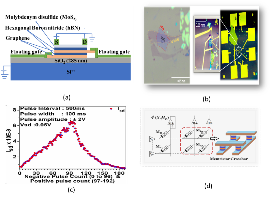
Fig. 3 | Memtransistor for low computational advantages
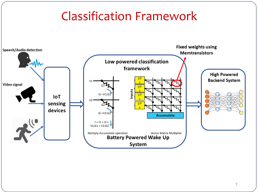
Fig. 4 | Memtransistor based classification framework
-
-
-
Kumar, Pratik, et al. “Neuromorphic In-Memory Computing Framework using Memtransistor Cross-bar based Support Vector Machines.” arXiv preprint arXiv:1903.12330 (2019).
-
-