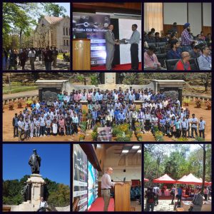
3rd India ESD Workshop (2019)
Venue: Faculty Hall, Main Building, IISc Bangalore
Date: 25th-26th Feb 2019 Hosted by: MSDLab @ Indian Institute of Science Bangalore
After successfully establishing its goals, in the first two editions, India ESD workshop (InEW) was back again with revamped 3rd edition. The one-year gap was useful in gathering more thoughts to make the event bigger and useful for wide range of audience for the ESD community in south Asia. InEW was envisioned by MSDLab @ IISc Bangalore (India) and ESD Association (USA) back in 2015, to promote the ESD design activities in India through a forum known as “India ESD Forum”. The four-fold vision of InEW is following (i) to increase ESD awareness among people working in the field of VLSI Microelectronics (ii) to bring engineers together who encounter ESD problems in their designs. (iii) to promote research, development and training related to on-chip ESD device/circuit design in India. (iv) Prominently use this model to strengthen Academia-Industry partnership in and around country. Unlike the previous editions, 3rd InEW is a two full day workshop with full length technical sessions and prominent invited speakers. The morning session of Day-1 started with opening remarks by Dr. Gianluca Boselli (Texas Instruments) on behalf of ESDA Board of Directors (BOD). He passed on the message of ESDA BOD and highlighted the need for such initiatives especially in southern Asia, and none better than Bangalore, which is known as Silicon Valley of India. The technical programme was kick started with Prof. Mayank Shrivastava (IISc Bangalore), with on chip ESD design essentials. The focus of this talk was to bring all the engineers on the same page as far as ESD design is concern. This session was followed by coffee break. It must be said that the live coffee served throughout the sessions helped audience to stay engaged in all sessions throughout. The second technical talk of the morning session of day-1 was from Dr. Gianluca, covering physics of different ESD protection devices and the impact of technology scaling on each of their design. This session was followed by the networking lunch where all the participants were seen in engaged technical discussions with each other in the lush green lawn. Post lunch session on Day-1 was packed with 20 min talks from ESD team leads from different Semiconductor companies based in both Bangalore and Singapore on miscellaneous ESD design issues at both chip and system level. This series of short lectures was followed by the poster sessions with round about 20 posters from both industry and academia again covering on-chip and system level ESD design topics along with novel materials and devices for ESD protection in beyond CMOS technologies. The evening session/final technical talk of day-1 was delivered by Dr. Charvaka Duvvury (IEEE Distinguished lecturer & Fellow) on CDM issues in high speed I/Os. This session was followed by gala dinner, where all the participants again got a chance to interact with speakers and students working on ESD get chance to directly interact with engineers from industry.