
ABSTRACT
This work presents the design and implementation of a six-channel software-defined oscilloscope on the STM32F407G-DISC1 Discovery board. The system employs dual simultaneous ADC sampling in REGSIMULT mode, with DMA-driven ping-pong buffering to capture six analog channels at up to 259kSps without CPU intervention during acquisition. A compact 14-byte binary UART frame protocol transmits synchronized six channel data to a host PC at 921600 baud, where a Python application built on matplotlib and pyserial renders live waveforms with per-channel statistics.
The firmware is developed in STM32CubeIDE using the HAL library and implements interrupt-driven UART command handling for pause and voltage-scale control. Starting from a text-based ASCII protocol at 115200 baud with software delays, the system was iteratively optimized to achieve a practical displayable frequency of approximately 300Hz, representing a roughly 50× improvement over the initial implementation. The project demonstrates the integration of ADC, DMA, UART, and GPIO peripherals in a real-time embedded data-acquisition pipeline.
I.INTRODUCTION
Oscilloscopes are indispensable instruments in electronics development, enabling engineers to observe voltage waveforms in the time domain. Commercial bench oscilloscopes, how ever, are costly and non-portable. Microcontroller-based software-defined oscilloscopes provide a low-cost alternative, trading bandwidth for flexibility and ease of customization.
The STM32F407G-DISC1 Discovery board is a capable platform for this purpose. Its ARM Cortex-M4 core running at 168MHz, triple 12-bit ADCs with hardware multi-mode support, and a general-purpose DMA controller make it well suited to real-time signal acquisition. When paired with a Python visualization front-end running on a host PC, the result is a complete end-to-end oscilloscope system requiring no dedicated display hardware on the embedded side.
The primary motivations for this project are:
• CPU-Free Acquisition: Employ DMA circular mode with ping-pong buffering so the CPU is never stalled waiting for ADC data, freeing it entirely for UART transmission.
• Multi-Channel Simultaneous Sampling: Use dual ADC REGSIMULT mode to sample six channels with zero phase skew between ADC1 and ADC2 pairs, essential for observing inter-channel phase relationships.
• High-Throughput Protocol Design: Replace a verbose ASCII serial protocol with a compact binary frame format, and raise the baud rate from 115200 to 921600, to achieve the highest possible displayable frequency within UART bandwidth constraints.
• Interactive Visualization: Implement a dark-theme Python GUI with per-channel toggle buttons, real-time Vpp statistics, and bidirectional UART command support for pause and voltage scaling.
II. BACKGROUND AND THEORY
2.1 Analog-to-Digital Conversion
The STM32F407 integrates three 12-bit successive approximation ADCs sharing a common reference voltage. Each ADC can be configured in scan mode with up to 16 conversion ranks, converting a sequence of input channels in a single triggered sweep. The conversion result is:
Vin = (raw / 4095 )×Vref (1)
where raw ∈[0,4095] and Vref =3.3V. With the ADC clock set to 21MHz (168MHz system clock, APB2 divide-by-2, ADC pre scaler divide-by-4) and a sampling time of 15 cycles, each conversion takes 15+12 = 27 ADC clock cycles.
2.2 Dual ADC Simultaneous Mode
ADC1 and ADC2 can be configured in REGSIMULT mode, in which both ADCs begin conversion simultaneously on the same trigger event. The DMA engine packs each pair of results into a single 32-bit word via ADC_DMAACCESSMODE 2:
word[n] = ADC2 result ≪16 ADC1 result (2)
This arrangement delivers six channel values per scan (three ranks each on ADC1 and ADC2) with no time skew between the paired channels, and halves the number of DMA transfers required compared to independent ADC operation.
2.3 DMA Ping-Pong Buffering
Direct Memory Access (DMA) transfers data between a peripheral and memory without CPU involvement. In circular mode, the DMA controller wraps around when it reaches the end of the configured buffer, generating two callbacks:
• Half-complete (HAL_ADC_ConvHalfCpltCallback): the first half of the buffer (PING) is filled and safe to read while DMA continues filling the second half.
• Full-complete (HAL_ADC_ConvCpltCallback): the second half (PONG) is filled and safe to read while DMA wraps and begins refilling the first half.
This double-buffering scheme guarantees uninterrupted acquisition: the CPU always reads from the half that DMA is not currently writing.
2.4 UART Throughput Analysis
UART transmits data serially at a fixed baud rate. Each byte requires 10 bits on the wire (1 start, 8 data, 1 stop) in 8N1 format. The maximum number of frames per second is:
Fmax= baud / 10×framebytes (3)
For a 14-byte binary frame at 921600 baud:
Fmax=921,600 / 10×14 ≈6,582frames/s (4)
Since each frame carries one sample set and a smooth waveform display requires at least 10 samples per cycle:
fdisplay=Fmax / 10 ≈658Hz (5)
This is the theoretical upper bound; in practice, Python processing over head limits the display able frequency to approximately 300Hz.
III.SYSTEM ARCHITECTURE
The complete system follows a five-stage pipeline from analog input to visual display:
Analog Signal → ADC(dual,21MHz) → DMA Buffer → UART (921600) → Python GUI
The STM32 firmware handles the first three stages entirely in hardware and interrupt context, with the main loop responsible only for framing and transmitting data. The Python application on the host PC handles the final two stages: frame parsing and waveform rendering at 25 frames per second.
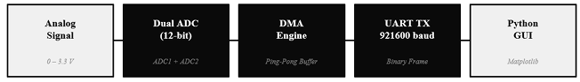
Figure 1: End-to-end system pipeline from analog signal input to Python waveform display
IV.HARDWARE DESCRIPTION
4.1 STM32F407G-DISC1 Discovery Board
The primary hardware platform is the STM32F407G-DISC1 Discovery kit. Its key specifications relevant to this project are: an ARM Cortex-M4 core at 168 MHz with hardware FPU, 1MB Flash,192 KB SRAM, three12 bit ADCs capable of up to2.4MSPS, two DMA controllers with eight streams each, and an onboard ST-Link/V2 debugger eliminating the need for an external programmer. The board is powered over USB and does not require an external supply.
4.2 Pin Connections
Table 1 lists all peripheral connections made to the STM32F407G-DISC1 for this project.
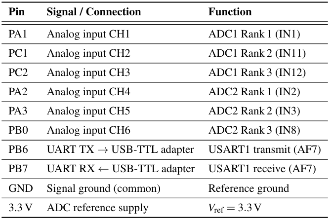
Table1:STM32F407G-DISC1 pin connection table
V.PERIPHERAL CONFIGURATION
5.1 ADC—Dual Simultaneous Mode
ADC1 is configured as the master in dual simultaneous regular mode (ADC_DUALMODEREG_SIMULT) with ADC_DMAACCESSMODE2. ADC 2 operates as the slave, triggered automatically a long side ADC1. Both ADCs are set to 12-bit resolution with right-aligned data, scan mode enabled, and continuous conversion mode active. Each ADC converts three channels(ranks), giving six channels total per scan. The sampling time for all channels is15cycles, reduced from the default 56 cycles to maximize throughput.
The sampling rate calculation is:
fADCclk = (168MHz / 2×4 ) =21MHz
tconv = (15+12 / 21MHz) =1.286µs
Rate = (21MHz / 27×3) ≈259kSps (6)
5.2 DMA—Circular Ping-Pong Buffer
DMA2 Stream 0 Channel 0 is assigned to ADC1 in circular mode. The buffer adc buffer [BUFFERSIZE] holds 60 32-bitwords (3sequences×10samples×2halves). On a half-complete interrupt, data ready is set to 1 (PING half ready); on a full-complete interrupt it is set to 2 (PONG half ready). The main loop reads the indicated half and clears the flag before UART transmission. DMA priority is set to highest to prevent buffer overruns.
5.3 USART1— Binary Frame Protocol
USART1 is configured at 921600 baud, 8N1, with no hardware flow control. GPIO pins PB6(TX) and PB7(RX) are configured as alternate function AF7 at very-highspeed. The overrun error flag(UART_FLAG_ORE) is checked and cleared in the main loop to prevent the UART from locking up at high data rates. Incoming command bytes are received via interrupt (HAL_UART_Receive_IT) and rearmed after each received byte.
VI.FIRMWARE DESIGN
6.1 Binary Frame Format
Each transmission consists of a 14-byte binary frame encoding six12-bit ADC values and a two-byte sync header. The frame structure is shown in Table 2.
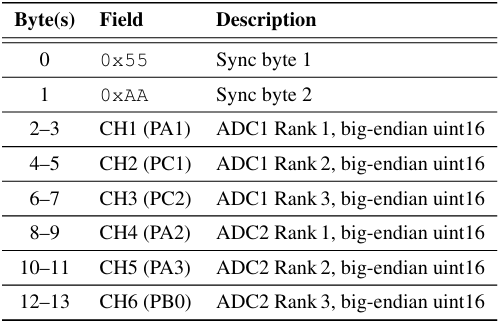
Table 2 : 14-byte binary UART frame format (big-endian)
The sync header 0x550xAA allows the Python parser to re-synchronize at any point by scanning for this two-byte pattern, making the protocol robust to partial frames at startup or after a buffer overrun.
6.2 32-BitWord Unpacking
In ADC_DMAACCESSMODE_2,each 32-bit DMA word packs two simultaneous ADC results:
word[n]=(ADC2result≪16) upper16bits | (ADC1result) lower16bits (7)
Unpacking in firmware:
ch1=word[0]&0xFFFF
ch4=(word[0]≫16)&0xFFFF (8)
The same pattern is applied for ranks 2 and 3 to recover all six channel values.
6.3 Command and Control Interface
The firmware implements two UART commands received via interrupt:
• ‘P’—Pause/Resume: Toggles the is paused flag. When paused, the main loop skips UART transmission but continues ADC and DMA operation, preserving the last displayed frame on the Python side.
• ‘S’—Scale: Toggles scale factor between 1 and 2. A factor of 2 multiplies all raw ADC values before framing, effectively doubling the displayed voltage range to 7.0V on the Python axis.
VII.PYTHON VISUALIZATION APPLICATION
7.1 Serial Frame Parser
The Python application accumulates incoming bytes in to a byte array buffer and scans for the 0x550xAA sync header before consuming a14-byte frame. For each valid frame, six 16-bit big-endian values are unpacked and converted to voltage.
V= raw×3.3 / 4095 (rawclampedto8190) (9)
Clamping to 8190 accommodates the scale ×2 firmware mode, which can push raw values above 4095.
7.2 Matplotlib Animation and GUI
The GUI is built with matplotlib and FuncAnimation. Six waveform lines are drawn on a dark-theme oscilloscope style axes, updated at 40ms intervals(25fps). The right panel displays per-channel peak-to-peak voltage (Vpp) statistics, updated on every animation frame.
A row of channel toggle buttons(CH1–CH6) allows individual channels to be shown or hidden. An ALL/NONE pair provides bulk control. A PAUSE button sends the ‘P’ command over serial and changes colour to indicate the paused state. A SCALE x2 button sends the ‘S’ command and adjusts the Y-axis limit from 3.5V to 7.0V.
TODO: Insert Python GUI screenshot (squarewave)here
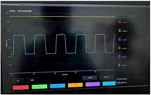
Figure 2 : Python oscilloscope GUI displaying a square wave on CH1. Channel toggle buttons, Vpp statistics panel, and PAUSE/SCALE controls are visible
VIII.IMPLEMENTATION CHALLENGES
8.1 Frequency Bottle neck: ASCII Protocol and Low Baud Rate
The initial firmware transmitted ADC readings as ASCII strings of the form CH1:1234|CH2:0567|…\r\n, consuming approximately 55 bytes per frame. At 115200baud with a HAL Delay(5) throttle inserted in the main loop, the effective frame rate was approximately100 frames per second, limiting the displayable waveform frequency to roughly 6–8Hz:
fdisplay, before= (∼100frames/s /10samples/cycle) ≈8Hz (10)
The fix involved three simultaneous changes: replacing the ASCII protocol with the14-byte binary frame, raising the baudrate to 921600, and removing HAL Delay entirely. The combined effect raised the frame rate to approximately 6582 frames per second and the practical displayable frequency to approximately 300Hz.
8.2 UART Overrun Error (ORE)
At 921600 baud, if the main loop is briefly delayed, the USART1 receive shift register receives a new byte before the previous one is read, setting the overrun error flag ORE. When ORE is set, the UART silently
discards subsequent bytes until the flag is cleared. The fix polls HALUARTGETFLAG(&huart1,UARTFLAGORE) in the main loop, clears it with HALUARTCLEAROREFLAG, and re-arms HAL UART Receive IT to restore command reception.
8.3 DMA Initialization Order
An early version of the firmware called MXADC1Init before MXDMA Init, which meant the DMA interrupt vector was not enabled when the ADC started. The result was that HAL_ADC_ConvHalfCpltCallback
and HAL_ADC_ConvCpltCallback never fired, leaving data ready permanently zero. The fix was to ensure MXDMA Init is always called before MXADC1Init in the Cube MX-generated initialization sequence.
8.4 Broken PA2 Board Trace
During early UART testing, the PA2 transmit pin on one of the Discovery boards was found to be non-functional due to a faulty PCB trace. Debugging was performed by confirming the fault with a loop back test and substituting an external USB-to-TTL adapter (CP2102) wired to alternative UART pins (PB6/PB7), which resolved the issue without requiring a board replacement.
8.5 ADC Sampling Time Tuning
The default 56-cycle sampling time per rank was retained from the Cube MX default, resulting in a scan rate of approximately 103kSps. Reducing the sampling time to 15 cycles increased the scan rate to 259kSps,removing any ADC-side bottle neck and ensuring the DMA buffer fills faster than UART can drain it.
IX.RESULTS AND OBSERVATIONS
9.1 Displayable Frequency
Table 3 summarises the before-and-after comparison of the key performance parameters following the protocol and baudrate optimizations.
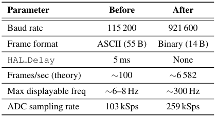
Table 3 : Performance comparison: initial vs. optimized implementation
9.2 Waveform Accuracy
Sine and square waves at frequencies up to approximately 300Hz were visually verified in the Python GUI by comparing the displayed period against the known signal generator frequency. The peak-to-peak voltage read out on the stats panel matched the applied signal amplitude within the expected quantization error of:
∆V= (3.3V / 4095) ≈0.806mV/LSB (11)
TODO: Insert Python GUI screen shot (sine wave at 300Hz) here
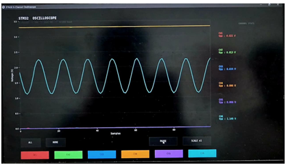
Figure 3 : Python oscilloscope GUI displaying a 300Hz sine wave on CH1. The Vpp read out in the stats panel confirms accurate amplitude measurement
9.3 Channel Isolation and Phase
With all six channels active, no cross-talk was observed between channels at the frequencies tested. The dual ADCREGSIMULT mode ensures that the paired channels (CH1/CH4, CH2/CH5, CH3/CH6) are sampled simultaneously with zero phase error, which was confirmed by driving two channels from the same signal source and observing perfectly overlapping waveforms on the display.
X.CONCLUSION AND FUTURESCOPE
This project successfully implements a six-channel real-time software oscilloscope on the STM32F407G-DISC1 Discovery board. Key outcomes are:
• DMA-Driven Acquisition: Circular ping-pong buffering with dual ADC simultaneous mode achieves 259kSps with zero CPU involvement during sampling, ensuring no samples are dropped regardless of UART transmission time.
• Binary Protocol Efficiency: Replacing the ASCII protocol with a 14-byte binary frame and raising the baudrate to 921600 produced a roughly 50× improvement in displayable frequency, from 6–8Hz to approximately
300Hz.
• Robust Synchronization: The two-byte sync header (0x550xAA) allows the Python parser to recover gracefully from any corrupted or partial frame, with no manual reset required.
• Interactive GUI: The Python application provides per channel toggle, real-time Vpp statistics, and bidirectional UART command support, demonstrating a complete embedded plus host-side system integration.
Future improvements include replacing UART with USB CDC (available on the STM32F407’s onboard USB OTG peripheral), which would raise the theoretical frame rate by over an order of magnitude and push the displayable frequency above 5kHz. Additional features such as hardware edge triggering, FFT frequency measurement overlay, and time-per division controls via onboard buttons are also planned.
REFERENCES
[1] STMicroelectronics, STM32F405/415, STM32F407/417, STM32F427/437 and STM32F429/439 Reference Manual,RM0090, Rev.19, 2021.
[2] STMicroelectronics, STM32F405xx / STM32F407xx Datasheet, DS8626, Rev.8, 2020.
[3] STMicroelectronics, Description of STM32F4 HAL and Low Layer Drivers, UM1725, Rev.8, 2020.
[4] STMicroelectronics, STM32’s ADC Modes and their Applications, Application Note AN3116, 2010.
[5] STMicroelectronics, Using the STM32F2, STM32F4 and STM32F7 Series DMA Controller, Application Note AN4031, 2016.
[6] ARM Limited, ARM Cortex-M4 Processor Technical Reference Manual, Revision r0p1, 2010.
[7] J. D. Hunter, “Matplotlib: A 2D graphics environment,” Computing in Science & Engineering, vol.9, no.3, pp.90–95, 2007.
Recent Comments