
ABSTRACT
This project presents the design and implementation of an adaptive low-power wireless sensor node built around theTM4C123GH6PM(TivaC)microcontroller, anESP8266Wi-Fimodule, and three analog sensors. The
system continuously monitors sensor data viaa12-bit ADC and publishes readings to an MQTT broker only when a significant change is detected, minimizing unnecessary wireless transmissions. A four-state Finite State Machine(FSM) governs power management, automatically escalating between Active, LightSleep, DeepSleep, and Hibernation modes based on sensor activity. UART-based communication drives the ESP8266 using AT commands, while a Node-RED dashboard visualizes live sensor data in real time. The proposed architecture achieves substantial power savings with no loss of sensing fidelity, making it well-suited for IoT applications such as remote environmental monitoring, industrial telemetry, and smart building automation.
I.INTRODUCTION
Wireless sensor nodes are fundamental building blocks of Internet of Things (IoT) infrastructure, deployed across domains ranging from environmental monitoring to industrial automation. A core challenge in such deployments is extending battery life while maintaining responsiveness to real-world events. Continuously operating a microcontroller and its radio at full power is energetically wasteful; equally, aggressive power-gating can introduce unacceptable latency or data loss.
This project implements an adaptive low-power wireless sensor node that addresses this trade-off using a hierarchical, event-driven power management strategy. The TM4C123GH6PM microcontroller samples three analog sensors at regular intervals via its built-in12-bit ADC. A four-state Finite State Machine(FSM)—Active, LightSleep, DeepSleep, and Hibernation automatically adjusts the operating mode based on observed sensor activity. When meaningful changes are detected (beyond a configurable threshold), the node wakes, processes the readings, and publishes them to an MQTT broker via an ESP8266 Wi-Fi module. A Node RED dashboard provides real-time visualization of all three sensor channels.
II.COMPONENTS USED
2.1 TM4C123GH6PM Microcontroller (TivaC LaunchPad)
The TM4C123GH6PM is a high-performance 32-bit ARM Cortex-M4F microcontroller from Texas Instruments, forming the central processing unit of this system. It handles ADC sampling, FSM-based power management, threshold detection, and serial communication with the ESP8266.
2.1.1 Key Features
•Core: ARM Cortex-M4F with floating-point unit
•Clock Speed: Up to 80MHz
•Flash Memory: 256KB
•SRAM: 32KB(retained during DeepSleep)
•ADC: Two12-bit ADC modules, up to 12 input channels,1MSPS
•Timers: Six 32/64-bit general-purpose timers
•UART: Eight UART modules
•Power Modes: Sleep, DeepSleep, and Hibernate (HIB module with RTC)
•OperatingVoltage: 3.3V
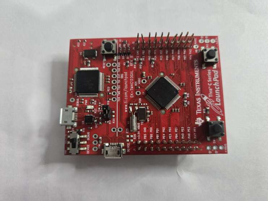
Figure 1: TM4C123GH6PM Tiva C LaunchPad
The Hibernate module is a key feature: it can power off the core and SRAM entirely, retaining only the RTC and a small register set, enabling a wake-on-RTC-match event. This enables the deepest power savings in the FSM.
2.2 ESP8266 Wi-Fi Module
The ESP8266 is a low-cost, low-power System-on-Chip (SoC) with a full TCP/IP stack and a 32-bit Tensilica L106 processor. In this project it is operated in AT-command mode, where the Tiva C sends standard Hayes AT commands over UART to connect to a Wi-Fi access point and publish MQTT messages.
2.2.1 Key Features
• Wi-Fi Standard: IEEE 802.11 b/g/n (2.4 GHz)
• Operating Voltage: 3.0–3.6 V
• UART Interface: Default baud rate 115200 (critical: 9600 causes garbled responses)
• Modes: Station (STA), Access Point (AP), or both (STA+AP)
• TCP/IP: Full stack onboard; supports AT+CIPSTART, AT+CIPSEND
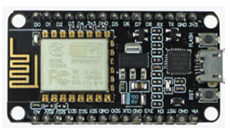
Figure 2: ESP8266 Wi-Fi Module
2.3 Analog Sensors
Three analog sensors are connected to the ADC input channels of the Tiva C:
• Potentiometer — connected to AIN0 (PE3): provides a continuously variable reference voltage, useful for simulating a generic analog process variable.
• Hall Effect Sensor — connected to AIN1 (PE2): detects magnetic field strength, applicable to current sensing or proximity detection.
• Light Sensor (LDR/Phototransistor)—connected to AIN2(PE1): measures ambient light intensity, enabling occupancy or day/night inference.
All three sensors output a 0–3.3 V analog signal, which is digitized by the 12-bit ADC to produce values in the range 0–4095.
2.4 MQTT Broker
MQTT (Message Queuing Telemetry Transport) is a lightweight publish-subscribe messaging protocol designed for constrained IoT devices. The node publishes sensor data to the topic tiva/data at QoS level 0. A local or cloud broker (e.g., HiveMQ) relays messages to all subscribers. The protocol’s minimal overhead makes it ideal for low-power, intermittent-connectivity nodes.
2.5 Node-RED Dashboard
Node-RED is a flow-based programming tool used here to subscribe to the MQTT topic, parse the JSON payload, and display live gauge values and trend charts for all three sensor channels. It runs on a PC or Raspberry Pi and requires no microcontroller-side changes to add new visualizations. It also supports easy integration with databases, cloud platforms, and alert systems for data logging and notifications. Additionally, its drag-and-drop interface allows rapid prototyping and customization of dashboards without deep programming knowledge.
2.6 Supporting Components
• Resistors and decoupling capacitors: for stable ADC references and UART signal integrity.
• Logic-level shifter (if required): the Tiva C operates at 3.3 V; the ESP8266 is also 3.3 V, so direct connection is safe.
• USB cable / external 3.3 V regulator: for powering the ESP8266, which can draw up to 300 mA during Wi-Fi transmission.
• Breadboard and connecting wires: for prototyping.
III.SYSTEM DESIGN
3.1 Block Diagram
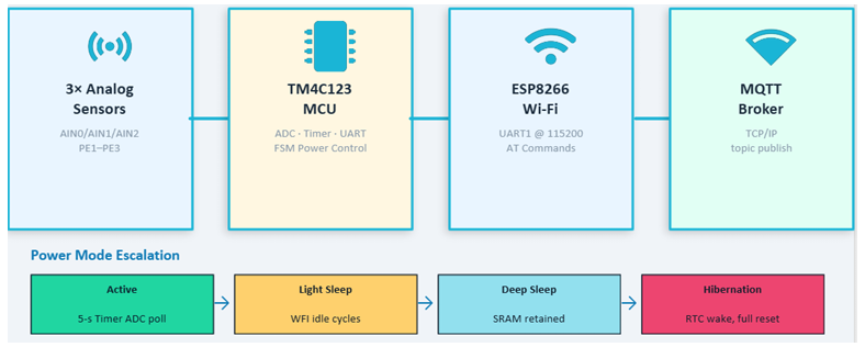
Figure 3: Block Diagram of Adaptive Low-Power Wireless Sensor Node
The system is structured as a pipeline: three analog sensors feed into the Tiva C’s ADC; the MCU processes readings and applies threshold logic; data passing the threshold is forwarded to the ESP8266 over UART; the ESP8266 publishes to an MQTT broker; and Node-RED subscribes and displays the data. Simultaneously, the FSM power manager observes activity levels and escalates or de-escalates the power mode accordingly.
3.2 Pin Mapping
The pin mapping for the implemented hardware setup is detailed below:
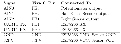
Table 1: Pin Mapping for Sensor Node
3.3 Working Principle
The system operates in a continuous loop governed by the FSM:
1. On power-up (or wake from Hibernation), all peripherals are initialized: ADC Sequencer 2, Timer0A, UART1, and the ESP8266 Wi-Fi/MQTT connection.
2. Timer0A fires an interrupt every 5 seconds, triggering an ADC conversion on all three channels (AIN0, AIN1,AIN2).
3. The ISR stores the new ADC readings and sets a new_sample_ready flag.
4. The main loop compares new readings against previous readings. If the absolute difference exceeds the threshold (150 ADC counts, ≈3.7% of full scale), the data is published via MQTT.
5. If no significant change is detected for LIGHT_SLEEP_LIMIT consecutive cycles, the FSM transitions to Light Sleep (WFI). Further inactivity causes escalation to Deep Sleep and then Hibernation.
6. Any sensor activity resets the FSM to Active mode.
IV.ADC SENSING AND TIMER ISR
4.1 ADC Configuration
The TM4C123 ADC is configured to use Sample Sequencer 2 (SS2), which supports up to four samples per trigger. Three channels — AIN0, AIN1, and AIN2 — are mapped to slots 0, 1, and 2 of the sequencer.
// ADC Sequencer 2 | 3 channels
ADC0_SSMUX2_R = 0x0210;
// slot0=AIN0, slot1=AIN1, slot2=AIN2
// END and IE only on the last slot
ADC0_SSCTL2_R = 0x0600;
// Trigger conversion (processor-initiated)
ADC0_PSSI_R |= 0x04;
while (!(ADC0_RIS_R & 0x04));
adc1 = ADC0_SSFIFO2_R;
adc2 = ADC0_SSFIFO2_R;
adc3 = ADC0_SSFIFO2_R;
The register SSCTL2 = 0x0600 sets the END and IE bits only on the third sample slot, ensuring a single interrupt fires after all three channels have been converted.
4.2 Timer ISR
Timer0A is configured for a 5-second periodic interrupt at an 80 MHz system clock:
• The timer reload value is set to 5×80,000,000 = 400,000,000 ticks. .
• The ISR triggers ADC SS2, waits for the conversion to complete, reads all three FIFO values, and sets new_sample_ready = 1
• The main loop polls new_sample_ready and invokes the threshold check and MQTT publish logic.
4.3 Threshold Logic
The change threshold is set to 150 ADC counts on the 12-bit scale (0–4095), corresponding to approximately 3.7% of full-scale range (150/4095 ≈ 3.66%). Only when any channel’s reading changes by more than this amount is an MQTT message published. This eliminates spurious transmissions due to sensor noise and reduces Wi-Fi wake-up events significantly.
V.FSM POWER MANAGEMENT
5.1 State Diagram
The power management is governed by a four-state FSM. Figure 4 shows the complete state transition diagram.
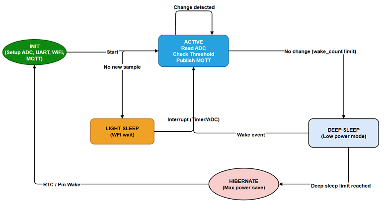
Figure 4: FSM State Transition Diagram for Power Mode Switching
5.2 State Descriptions
5.2.1 Active Mode
• Timer0A fires every 5 seconds.
• ADC SS2 samples all three sensors.
• If |∆ADC| > 150, MQTT publish is invoked and wake_count is reset to 0.
• If no significant change is detected, wake_count increments; once it reaches LIGHT_SLEEP_LIMIT, the FSM transitions to Light Sleep.
5.2.2 Light Sleep (WFI)
• The CPU is halted via the ARM WFI (Wait for Interrupt) instruction.
• All peripherals (ADC, Timer, UART) remain clocked.
• Timer0A still fires every 5 seconds, waking the CPU to check sensors.
• After LIGHT_SLEEP_LIMIT consecutive idle timer wakes, the FSM escalates to Deep Sleep.
5.2.3 Deep Sleep
- The ARM SLEEPDEEP bit is set in the System Control Register (SCR).
- The deep-sleep clock configuration reduces peripheral clocking to the PIOSC (16 MHz internal oscillator), turning off the PLL and MOSC.
- SRAM is retained — variables such as deep sleep count and previous ADC readings survive this mode.
- Awake event (Timer0A or GPIO interrupt) returns the system to Active mode.
- After two entries into Deep Sleep without activity, the FSM transitions to Hibernation.
5.2.4 Hibernation
• The Hibernate module fully powers off the core, all peripherals, and SRAM.
• The RTC match register is loaded with a 60-second wake interval.
• Hibernation is initiated by setting the HIBREQ bit in HIB_CTL_R.
• Wake occurs as a full system reset; HIB_RIS_R is checked to distinguish a hibernation wake from a cold power-on.
5.3 Power Mode Comparison Table
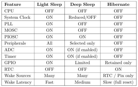
Table 2: Comparison of Power Modes on TM4C123GH6PM
VI.MQTT AND ESP8266 COMMUNICATION
6.1 UART1 Configuration
UART1 is used to communicate with the ESP8266 at 115200 baud. The baud rate divisor (BRD) is calculated from:

Thus IBRD = 8 and FBRD = round(0.68×64) = 44.
// UART1 | 115200 baud @ 16 MHz
UART1_IBRD_R = 8;
UART1_FBRD_R = 44;
// 8-bit, no parity, 1 stop bit, FIFO enabled
UART1_LCRH_R = 0x70;
// Enable UART, TX, and RX
UART1_CTL_R = 0x301;
Note: Operating the ESP8266 at 9600 baud causes garbled AT-command responses and communication hangs. Always use 115200 baud.
6.2 AT Command Sequence
The Tiva C communicates with the ESP8266 using Hayes AT commands over UART1:
1. AT+RST — reset the module
2. AT+CWMODE=1 — set to Station mode
3. AT+CWJAP= “SSID”,” password” — join the Wi-Fi network
4. AT+CIPSTART=”TCP”,”broker_ip”,1883 — open TCP connection to MQTT broker
5. AT+CIPSEND=N — declare N bytes to send
6. Raw MQTT CONNECT packet — establish MQTT session
7. Raw MQTT PUBLISH packet — publish sensor data
6.3 MQTT Packet Flow
The MQTT session follows the standard publish workflow at QoS level 0:
• CONNECT→broker (client ID, keepalive)
• CONNACK←broker (return code 0 = accepted)
• PUBLISH → broker on topic tiva/data, payload: JSON string with all three ADC values
The JSON payload format is:
{“s1”: 2847, “s2”: 1563, “s3”: 3102}
6.4 Communication Flow Diagram
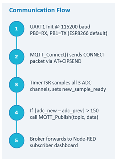
Figure 5: End-to-end Communication Flow: Sensors → Tiva C → ESP8266 → MQTT → Node-RED
VII.NODE-RED DASHBOARD
7.1 Overview
Node-RED subscribes to the MQTT topic tiva/data and parses the incoming JSON payload. Each of the three sensor values is routed to a separate gauge widget and a trend chart, providing a real-time visual overview of all channels.
7.2 Dashboard Layout
• Sensor 1 (Potentiometer / AIN0 / PE3): Gauge displays 0–4095 ADC range; trend chart shows last 60 readings.
• Sensor 2 (Hall Effect / AIN1 / PE2): Gauge displays 0–4095; chart highlights magnetic field events.
• Sensor 3 (Light Sensor / AIN2 / PE1): Gauge shows ambient light level; chart enables day/night pattern analysis.
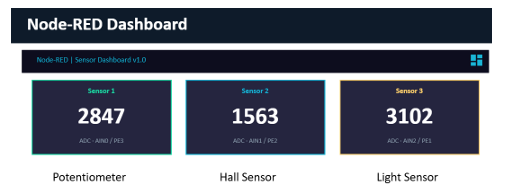
Figure 6: Node-RED Dashboard showing live ADC readings for all three sensor channels
VIII.IMPLEMENTATION
8.1 ADC and Timer
• Enable ADC0 clock via SYSCTL_RCGCADC_R.
• Configure PE1–PE3 as analog inputs (disable digital function via GPIODEN).
• Set SS2 sequencer with SSMUX2 = 0x0210 and SSCTL2 = 0x0600.
• Configure Timer0A for 5-second periodic interrupts at 80 MHz.
• Enable Timer0A interrupt in NVIC; ISR reads all three FIFO values.
8.2 UART1 (ESP8266)
• UART1 TX → PB1 (connect to ESP8266 RX)
• UART1 RX →PB0 (connect to ESP8266 TX)
• Baud rate: 115200, 8N1
• VCC →3.3 V (dedicated regulator recommended for ESP8266)
• GND →GND(common ground with Tiva C)
8.3 Analog Sensors
• Potentiometer wiper → PE3 (AIN0); ends to 3.3 V and GND
• Hall Effect Sensor output → PE2 (AIN1); VCC to 3.3 V, GND to GND
• Light Sensor output → PE1 (AIN2); VCC to 3.3 V, GND to GND
8.4 Power Supply
• The Tiva C LaunchPad is powered via USB (5 V regulated to 3.3 V on-board).
• TheESP8266 requires up to 300 mA peak during Wi-Fi transmission; an external 3.3 V regulator (e.g., AMS1117 3.3) with adequate bulk capacitance is recommended.
• A common ground reference is maintained across all components.
IX.RESULTS
9.1 Functional Verification
• All three ADC channels correctly sampled every 5 seconds via Timer0A ISR.
• Threshold-based publishing confirmed: MQTT messages transmitted only when |∆ADC| > 150 counts, significantly reducing Wi-Fi events during stable conditions.
• FSM transitions verified: Active → Light Sleep → Deep Sleep → Hibernation observed sequentially during sensor inactivity; automatic return to Active upon sensor change confirmed.
• SRAM variable deep_sleep_count correctly retained across Deep Sleep cycles and reset to zero after Hibernation (full power-off).
• UART1 at 115200 baud: clean AT-command responses and successful MQTT CONNECT/PUBLISH; 9600 baud caused garbled communication (confirmed and corrected during debugging).
9.2 Hardware Setup
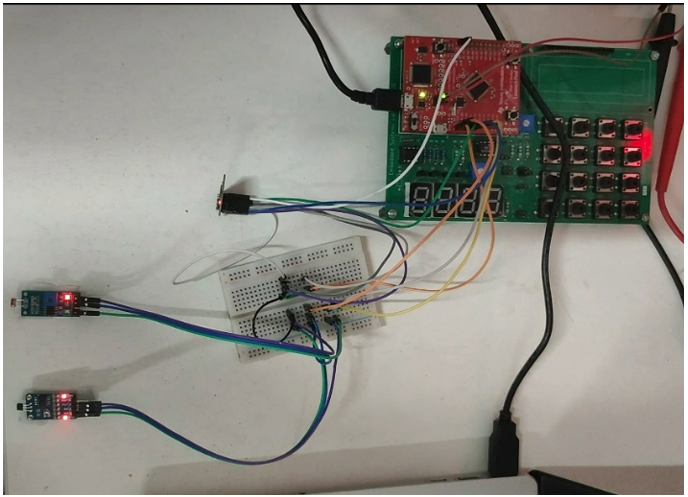
Figure 7: Hardware Setup — Tiva C, ESP8266, and three analog sensors on breadboard
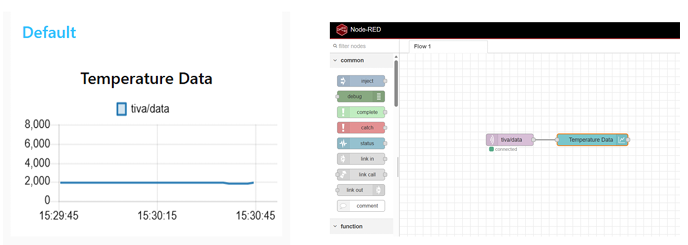
Figure 8: Live Node-RED Dashboard with real-time sensor readings
X.APPLICATIONS
• Remote environmental monitoring: temperature, humidity, and light sensing in battery-powered outdoor nodes.
• Industrial telemetry: monitoring machine vibration or magnetic fields with minimal cabling, powered by energy harvesting.
• Smart building automation: occupancy-based lighting and HVAC control using light and Hall-effect sensors.
• Agricultural IoT: soil moisture or sunlight monitoring in field-deployed sensor networks.
• Asset tracking: low-power nodes reporting status periodically, hibernating between events.
XI.CONCLUSION
The Adaptive Low-Power Wireless Sensor Node demonstrates an effective strategy for balancing sensing responsiveness and energy conservation in an IoT context. By combining a hierarchical four-state power FSM with threshold based MQTT publishing, the system avoids continuous high-power operation without sacrificing data fidelity. The TM4C123GH6PM’s ADC, timer, and Hibernate module prove well-suited for this role, offering flexible power-mode control and SRAM retention across intermediate sleep states.
The ESP8266 provides a cost-effective Wi-Fi front-end, and the MQTT protocol’s lightweight footprint minimizes on-air time. Node-RED’s flow-based dashboard enables rapid prototyping of visualization and alerting logic without modifying the embedded firmware.
The modular architecture allows straightforward extension: additional sensors can be added to the remaining ADC channels, the MQTT topic structure can be expanded, and the power thresholds can be tuned for specific deployment environments. This makes the platform a strong foundation for production-grade IoT sensor nodes in energy-constrained applications.
REFERENCES
[1] Texas Instruments, TM4C123GH6PM Microcontroller Datasheet, 2014. Available: https://www.ti.com/product/TM4C123GH6PM
[2] Texas Instruments, Tiva™ C Series TM4C123G LaunchPad Evaluation Board User’s Guide, SPMU296, 2013.
[3] Espressif Systems, ESP8266 AT Instruction Set, Version 2.2.0, 2019.
[4] OASIS Standard, MQTT Version 3.1.1, 2014. Available: https://mqtt.org/mqtt-specification/
[5] Node-RED Project, Node-RED Documentation, 2023. Available: https://nodered.org/docs/
Recent Comments