
| USING PLL | SAMPLE | TASKS |
TM4C123GH6PM MCU has four different clock sources:
- Precision Internal Oscillator (PIOSC) : 16 MHz.
- Main Oscillator (MOSC) : It can use an external clock source or an external crystal.
- Low-Frequency Internal Oscillator (LFIOSC) : An on-chip internal 30 kHz Oscillator used for Deep-Sleep power-saving modes.
- Hibernate RTC Oscillator (RTCOSC) : It can be configured to be the 32.768 KHz external oscillator source from the Hibernation (HIB) module or the HIB Low-Frequency clock source (HIB LFIOSC), which is intended to provide the system with a real-time clock source.
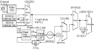
The system clock is generated by a PLL that can be driven by any crystals or oscillators running between 5 and 25 MHz. The output frequency of the PLL is always 400 MHz, and it is independent on the input clock sources.
Two clock sources, Main OSC (MOSC) and Precision Internal osc (PIOSC) 16 MHz, can work as a clock source for the PLL, and this source can be selected via the MUX. Two multiplexers (MUXs) are used to select different clock sources, and two ways can be used to create a system clock to be used by the CPU:
- One way is to use the Phase-Locked Loop (PLL) clock generator that needs a clock source as the input source to create this system clock.
- Another way is to directly use any one of four clock sources, and this can be selected via a MUX. An easy way is to use Precision Internal OSC (16 MHz) divided by 4 to get a 4-MHz system clock.
When using the PLL, the output frequency of 400 MHz is pre-divided by 2 (becomes 200 MHz) before the user’s divisor is applied. Users can modify this 200-MHz system clock by adding different dividing factors in the SYSDIV in their program to use a lower-frequency system clock. The selected clock source can avoid the SYSDIV and USESYSDIV dividing operations via BYPASS for both MUXs and can be directly sent out as the system clock.
Two registers, Run-Mode Clock Configuration (RCC) register and Run-Mode Clock Configuration 2 (RCC2) register, provide controls for the system clock. The RCC2 register is used to provide additional control parameters that offer additional encodings over the RCC register. These registers control the following clock functionality:
- Source of clocks in sleep and deep-sleep modes
- System clock derived from PLL or other clock source
- Enable or disable the oscillators and PLL
- Clock divisors
- Crystal input selection
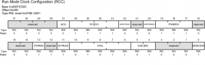
Run-Mode Clock Configuration

| Bit Number |
Bit Name |
Bit Function |
|---|---|---|
| 0 | MOSCDIS | 0: The main oscillator is enabled 1: The main oscillator is disabled—Default |
| 5-4 | OSCSRC | Oscillator Source Selection: 0x0: Main Oscillator (MOSC) 0x1: Precision Internal Oscillator (PIOSC)—Default 0x2: Precision Internal Oscillator/4 (PIOSC/4) 0x3: Low-Frequency Internal Oscillator (LFIOSC) |
| 11 | BYPASS | 0: The system clock uses the PLL output clock divided by the divisor specified by SYSDIV (bits 26–23 in this register) 1: The system clock uses the OSC source and divided by the divisor specified by SYSDIV (bits 26–23 in this register) |
| 13 | PWRDN | 0: The PLL is operating normally 1: The PLL is powered down. Make sure that another clock source is functioning and that the BYPASS bit is set before setting this bit |
| 22 | USESYSDIV | 0: The system clock is used undivided 1: The system clock divider is used for the system clock. The system clock divider is forced to be used when the PLL is selected as the source |
| 26-23 | SYSDIV | System Clock Divisor Specifies which divisor is used to generate the system clock from either the PLL output or from the oscillator source, depending on how the BYPASS bit in this register is configured. |
| 27 | ACG | 0: The Run-Mode Clock Gating Control (RCGCn) registers are used when the microcontroller enters a sleep mode 1: The SCGCn or DCGCn registers are used to control the clocks distributed to the peripherals when the microcontroller is in a sleep mode. |
In the RCC register, the SYSDIV field specifies which divisor is used to generate the system clock from either the PLL output or the oscillator source. When using the PLL, the VCO frequency of 400 MHz is pre-divided by 2 before the divisor is applied.
| SYSDIV | DIVISOR | Frequency BYPASS=0 |
Frequency BYPASS=1 |
Symbolic Definition (Tivaware) |
|---|---|---|---|---|
| 0x0 | ÷1 | Reserved | Clock source frequency/1 | SYSCTL_SYSDIV_1 |
| 0x1 | ÷2 | Reserved | Clock source frequency/2 | SYSCTL_SYSDIV_2 |
| 0x2 | ÷3 | 66.67 MHz | Clock source frequency/3 | SYSCTL_SYSDIV_3 |
| 0x3 | ÷4 | 50 MHz | Clock source frequency/4 | SYSCTL_SYSDIV_4 |
| 0x4 | ÷5 | 40 MHz | Clock source frequency/5 | SYSCTL_SYSDIV_5 |
| 0x5 | ÷6 | 33.33 MHz | Clock source frequency/6 | SYSCTL_SYSDIV_6 |
| 0x6 | ÷7 | 28.57 MHz | Clock source frequency/7 | SYSCTL_SYSDIV_7 |
| 0x7 | ÷8 | 25 MHz | Clock source frequency/8 | SYSCTL_SYSDIV_8 |
| 0x8 | ÷9 | 22.22 MHz | Clock source frequency/9 | SYSCTL_SYSDIV_9 |
| 0x9 | ÷10 | 20 MHz | Clock source frequency/10 | SYSCTL_SYSDIV_10 |
| 0xA | ÷11 | 18.18 | Clock source frequency/11 | SYSCTL_SYSDIV_11 |
| 0xB | ÷12 | 16.67 MHz | Clock source frequency/12 | SYSCTL_SYSDIV_12 |
| 0xC | ÷13 | 15.38 MHz | Clock source frequency/13 | SYSCTL_SYSDIV_13 |
| 0xD | ÷14 | 14.29 MHz | Clock source frequency/14 | SYSCTL_SYSDIV_14 |
| 0xE | ÷15 | 13.33 MHz | Clock source frequency/15 | SYSCTL_SYSDIV_15 |
| 0xF | ÷16 | 12.5 MHz Default |
Clock source frequency/16 | SYSCTL_SYSDIV_16 |
The XTAL (bits 6-10) field specifies Crystal Frequency and is given in the following table.
| XTAL | Crystal Freq (MHz) | XTAL | Crystal Freq (MHz) | XTAL | Crystal Freq (MHz) |
|---|---|---|---|---|---|
| 0x4 | 3.579545 MHz | 0xC | 6.144 MHz | 0x14 | 14.31818 MHz |
| 0x5 | 3.6864 MHz | 0xD | 7.3278 MHz | 0x15 | 16.0 MHz |
| 0x06 | 4 MHz | 0xE | 8 MHz | 0x16 | 16.384 MHz |
| 0x7 | 4.096 MHz | 0xF | 8.192 MHz | 0x17 | 18.0 MHz |
| 0x8 | 4.9152 MHz | 0x10 | 10.0 MHz | 0x18 | 20.0 MHz |
| 0x9 | 5 MHz | 0x11 | 12.0 MHz | 0x19 | 24.0 MHz |
| 0xA | 5.12 MHz | 0x12 | 12.288 MHz | 0x1A | 25.0 MHz |
| 0xB | 6 MHz (reset value) | 0x13 | 13.56 MHz | others | reserved |
Run-Mode Clock Configuration 2
| Bit Number |
Bit Name |
Bit(s) Function |
|---|---|---|
| 6-4 | OSCSRC2 | Oscillator Source 2 (Selects the input source for the OSC) 0x0: MOSC (Main oscillator) 0x1: PIOSC (Precision internal oscillator) 0x2: PIOSC/4 (Precision internal oscillator / 4) 0x3: LFIOSC (Low-frequency internal oscillator) 0x4 – 0x6: Reserved 0x7: 32.768 kHz (32.768-kHz external oscillator) |
| 11 | BYPASS2 | PLL Bypass 2 0: The system clock is the PLL output clock divided by the divisor specified by SYSDIV2. 1: The system clock is derived from the OSC source and divided by the divisor specified by SYSDIV2. |
| 13 | PWRDN2 | Power-Down PLL 2 0: The PLL operates normally 1: The PLL is powered down. |
| 22 | SYSDIV2LSB | Additional LSB for SYSDIV2 When DIV400 is set, this bit becomes the LSB of SYSDIV2. If DIV400 is clear, this bit is not used. This bit can only be set or cleared when DIV400 is set. |
| 28-23 | SYSDIV2 | System Clock Divisor 2 Specifies which divisor is used to generate the system clock from either the PLL output or the oscillator source. SYSDIV2 is used for the divisor when both the USESYSDIV bit in the RCC register and the USERCC2 bit in this register are set. |
| 30 | DIV400 | Divide PLL as 400 MHz versus 200 MHz This bit, along with the SYSDIV2LSB bit, allows additional frequency choices. 0: Use SYSDIV2 as is and apply to 200 MHz predivided PLL output. 1: Append the SYSDIV2LSB bit to the SYSDIV2 field to create a 7 bit divisor using the 400 MHz PLL output. |
| 31 | USERCC2 | Use RCC2 0: The RCC register fields are used, and the fields in RCC2 are ignored. 1: The RCC2 register fields override the RCC register fields. |
The RCC2 provides extend fields and functions compared with the RCC register. The SYSDIV2 field in the RCC2 register is 2 bits wider than the SYSDIV field in the RCC register so that additional larger divisors up to 64 are available to allow a lower system clock frequency to be used to improve the system Deep Sleep power consumption. The following Table shows how the SYSDIV2 encoding affects the system clock frequency, depending on whether the PLL is used (BYPASS2=0) or another clock source is used (BYPASS2=1).
When the RCC2 is used, it will override the functions provided by the RCC register.
| SYSDIV2 | DIVISOR | Frequency BYPASS2=0 |
Frequency BYPASS2=1 |
Symbolic Definition (Tivaware) |
|---|---|---|---|---|
| 0x0 | ÷1 | Reserved | Clock source frequency/1 | SYSCTL_SYSDIV_1 |
| 0x1 | ÷2 | Reserved | Clock source frequency/2 | SYSCTL_SYSDIV_2 |
| 0x2 | ÷3 | 66.67 MHz | Clock source frequency/3 | SYSCTL_SYSDIV_3 |
| 0x3 | ÷4 | 50 MHz | Clock source frequency/4 | SYSCTL_SYSDIV_4 |
| 0x4 | ÷5 | 40 MHz | Clock source frequency/5 | SYSCTL_SYSDIV_5 |
| … | … | … | …. | … |
| 0x9 | ÷10 | 20 MHz | Clock source frequency/10 | SYSCTL_SYSDIV_10 |
| … | … | … | … | … |
| 0x3F | ÷64 | 3.125 MHz | Clock source frequency/64 | SYSCTL_SYSDIV_64 |
Raw Interrupt Status (RIS)
Programming the PLL
The Main Oscillator (MOSC) for the TM4C on the evaluation board is 16 MHz. This means the reference clock (Ref Clk) input to the phase/frequency detector will be 16 MHz. For a 16 MHz crystal, we set the XTAL bits to 10101 (0x15). We use RCC2 because it provides more options
- Configure the system to use RCC2 (SYSCTL_RCC2_R)for advanced features. If the RCC2 register is being used, the USERCC2 bit must be set and the appropriate RCC2 bit/field is used.
- Set BYPASS2 (bit 11), thereby configuring the microcontroller to run off a “raw” clock source and following for the new PLL configuration to be validated before switching the system clock to the PLL.
- Specify the crystal frequency in the four XTAL bits. The OSCSRC2 bits are cleared to select the main oscillator as the oscillator clock source.
- Clear PWRDN2 (bit 13) to activate the PLL.
- Configure and enable the clock divider using the 7-bit SYSDIV2 field. If the 7-bit SYSDIV2 is n, then the clock will be divided by n+1. To get the desired 80 MHz from the 400 MHz PLL, we need to divide by 5. So, we place a 4 into the SYSDIV2 field.
- Wait for the PLL to stabilize by waiting for PLLRIS (bit 6) in the SYSCTL_RIS_R to become high.
- Connect the PLL by clearing the BYPASS2 bit.
Recent Comments