
If the timers are only used for the timing-base or timing-up indications, one does not need to use these Capture/Compare pins (CCP) since these pins are mainly connected to the external signals to detect the number of events that have occurred or the time period events that have been experienced.
In the previous session, we showed how to use timers to generate time delay. In this lab session, we will examine the use of timers with the I/O pins. There are five modes for each timer block. They are :
- One-shot/Periodic mode,
- Real-time clock mode,
- Input edge-time mode,
- Input edge-count mode and
- Pulse Width Modulation (PWM).
TimerA and TimerB CCP pins
There are TimerA and TimerB for each of the Timer block 0 to 5. There are one or two designated pins for each of the TimerA and TimerB. For example, TimerA of Timer block 4 is connected internally to pin PC0 of PortC and TimerB of Timer block 4 is connected to pin PC1 of PortC. Notice, TimerA pins are also called CCP0 and TimerB pins are called CCP1. Some of the timers have option to be connected to one of the two pins. For example, TimerA of Timer1 (T1CCP0) can use PB0 or PF2 pins. Table 9.1 shows the pin designations for 16/32-bit Timer block 0 to 5.
| TimerA | Pins | TimerB | Pins | |
|---|---|---|---|---|
| Timer0 | T0CCP0 | PB6 or PF0 | T0CCP1 | PB7 or PF1 |
| Timer1 | T1CCP0 | PB4 or PF2 | T1CCP1 | PB5 or PF3 |
| Timer2 | T2CCP0 | PB0 or PF4 | T2CCP1 | PB1 |
| Timer3 | T3CCP0 | PB2 | T3CCP1 | PB3 |
| Timer4 | T4CCP0 | PC0 | T4CCP1 | PC1 |
| Timer5 | T5CCP0 | PC2 | T5CCP1 | PC3 |
General-Purpose Timers CCP pins distributions
| Timer Pin | I/O pin | Pin Function |
|---|---|---|
| T0CCP0 | PB6 | 16/32-Bit Timer 0 Capture/Compare/PWM 0 |
| PF0 | ||
| T0CCP1 | PB7 | 16/32-Bit Timer 0 Capture/Compare/PWM 1 |
| PF1 | ||
| T1CCP0 | PB4 | 16/32-Bit Timer 1 Capture/Compare/PWM 0 |
| PF2 | ||
| T1CCP1 | PB5 | 16/32-Bit Timer 1 Capture/Compare/PWM 1 |
| PF3 | ||
| T2CCP0 | PB0 | 16/32-Bit Timer 2 Capture/Compare/PWM 0 |
| PF4 | ||
| T2CCP1 | PB1 | 16/32-Bit Timer 2 Capture/Compare/PWM 1 |
| T3CCP0 | PB2 | 16/32-Bit Timer 3 Capture/Compare/PWM 0 |
| T3CCP1 | PB3 | 16/32-Bit Timer 3 Capture/Compare/PWM 1 |
| T4CCP0 | PC0 | 16/32-Bit Timer 4 Capture/Compare/PWM 0 |
| T4CCP1 | PC1 | 16/32-Bit Timer 4 Capture/Compare/PWM 1 |
| T5CCP0 | PC2 | 16/32-Bit Timer 5 Capture/Compare/PWM 0 |
| T5CCP1 | PC3 | 16/32-Bit Timer 5 Capture/Compare/PWM 1 |
| WT0CCP0 | PC4 | 32/64-Bit Wide Timer 0 Capture/Compare/PWM 0 |
| WT0CCP1 | PC5 | 32/64-Bit Wide Timer 0 Capture/Compare/PWM 1 |
| WT1CCP0 | PC6 | 32/64-Bit Wide Timer 1 Capture/Compare/PWM 0 |
| WT1CCP1 | PC7 | 32/64-Bit Wide Timer 1 Capture/Compare/PWM 1 |
| WT2CCP0 | PD0 | 32/64-Bit Wide Timer 2 Capture/Compare/PWM 0 |
| WT2CCP1 | PD1 | 32/64-Bit Wide Timer 2 Capture/Compare/PWM 1 |
| WT3CCP0 | PD2 | 32/64-Bit Wide Timer 3 Capture/Compare/PWM 0 |
| WT3CCP1 | PD3 | 32/64-Bit Wide Timer 3 Capture/Compare/PWM 1 |
| WT4CCP0 | PD4 | 32/64-Bit Wide Timer 4 Capture/Compare/PWM 0 |
| WT4CCP1 | PD5 | 32/64-Bit Wide Timer 4 Capture/Compare/PWM 1 |
| WT5CCP0 | PD6 | 32/64-Bit Wide Timer 5 Capture/Compare/PWM 0 |
| WT5CCP1 | PD7 | 32/64-Bit Wide Timer 5 Capture/Compare/PWM 1 |
Selecting alternate function for Timers pin
Upon Reset, the GPIOAFSEL register has all 0s meaning the I/O pins are used as simple I/O. To use an alternate function, we first must set the bit in the AFSEL register to 1 for that pin. For example, for the PB6, we need to write 0x40 to GPIO_PORTB_AFSL_R register. After that, the GPIOPCTL register must be configured for the desired function. To do that, we need to use the information in Table 23-5 (Page No.1351) of TI Tiva TM4C123GH6PM data sheet .
Table 9.2 provides the summary for the Timers pins.
| Timer Pin | I/O pin | How to use peripheral function on the pin |
|---|---|---|
| T0CCP0 | PB6 | GPIO_PORTB_AFSEL_R = 0x40 |
| PF0 | GPIO_PORTF_AFSEL_R = 0x01 | |
| T0CCP1 | PB7 | GPIO_PORTB_AFSEL_R = 0x80 |
| PF1 | GPIO_PORTF_AFSEL_R = 0x02 | |
| T1CCP0 | PB4 | GPIO_PORTB_AFSEL_R = 0x10 |
| PF2 | GPIO_PORTF_AFSEL_R = 0x04 | |
| T1CCP1 | PB5 | GPIO_PORTB_AFSEL_R = 0x20 |
| PF3 | GPIO_PORTF_AFSEL_R = 0x08 | |
| T2CCP0 | PB0 | GPIO_PORTB_AFSEL_R = 0x40 |
| PF4 | GPIO_PORTF_AFSEL_R = 0x10 | |
| T2CCP1 | PB1 | GPIO_PORTB_AFSEL_R = 0x02 |
| T3CCP0 | PB2 | GPIO_PORTB_AFSEL_R = 0x04 |
| T3CCP1 | PB3 | GPIO_PORTB_AFSEL_R = 0x08 |
| T4CCP0 | PC0 | GPIO_PORTC_AFSEL_R = 0x01 |
| T4CCP1 | PC1 | GPIO_PORTC_AFSEL_R = 0x02 |
| T5CCP0 | PC2 | GPIO_PORTC_AFSEL_R = 0x04 |
| T5CCP1 | PC3 | GPIO_PORTC_AFSEL_R = 0x08 |
| WT0CCP0 | PC4 | GPIO_PORTC_AFSEL_R = 0x10 |
| WT0CCP1 | PC5 | GPIO_PORTC_AFSEL_R = 0x20 |
| WT1CCP0 | PC6 | GPIO_PORTC_AFSEL_R = 0x40 |
| WT1CCP1 | PC7 | GPIO_PORTC_AFSEL_R = 0x80 |
| WT2CCP0 | PD0 | GPIO_PORTD_AFSEL_R = 0x01 |
| WT2CCP1 | PD1 | GPIO_PORTD_AFSEL_R = 0x02 |
| WT3CCP0 | PD2 | GPIO_PORTD_AFSEL_R = 0x04 |
| WT3CCP1 | PD3 | GPIO_PORTD_AFSEL_R = 0x04 |
| WT4CCP0 | PD4 | GPIO_PORTD_AFSEL_R = 0x10 |
| WT4CCP1 | PD5 | GPIO_PORTD_AFSEL_R = 0x20 |
| WT5CCP0 | PD6 | GPIO_PORTD_AFSEL_R = 0x40 |
| WT5CCP1 | PD7 | GPIO_PORTD_AFSEL_R = 0x80 |
| Timer Pin | I/O pin | How to select the timer function on the pin |
|---|---|---|
| T0CCP0 | PB6 | GPIO_PORTB_PCTL_R = 0x0700.0000 |
| PF0 | GPIO_PORTF_PCTL_R = 0x0000.0007 | |
| T0CCP1 | PB7 | GPIO_PORTB_PCTL_R = 0x7000.0000 |
| PF1 | GPIO_PORTF_PCTL_R = 0x0000.0070 | |
| T1CCP0 | PB4 | GPIO_PORTB_PCTL_R = 0x0007.0000 |
| PF2 | GPIO_PORTF_PCTL_R = 0x0000.0700 | |
| T1CCP1 | PB5 | GPIO_PORTB_PCTL_R = 0x0070.0000 |
| PF3 | GPIO_PORTF_PCTL_R = 0x0000.7000 | |
| T2CCP0 | PB0 | GPIO_PORTB_PCTL_R = 0x0000.0007 |
| PF4 | GPIO_PORTF_PCTL_R = 0x0007.0000 | |
| T2CCP1 | PB1 | GPIO_PORTB_PCTL_R = 0x0000.0070 |
| T3CCP0 | PB2 | GPIO_PORTB_PCTL_R = 0x0000.0700 |
| T3CCP1 | PB3 | GPIO_PORTB_PCTL_R = 0x0000.7000 |
| T4CCP0 | PC0 | GPIO_PORTC_PCTL_R = 0x0000.0007 |
| T4CCP1 | PC1 | GPIO_PORTC_PCTL_R = 0x0000.0070 |
| T5CCP0 | PC2 | GPIO_PORTC_PCTL_R = 0x0000.0700 |
| T5CCP1 | PC3 | GPIO_PORTC_PCTL_R = 0x0000.7000 |
| WT0CCP0 | PC4 | GPIO_PORTC_PCTL_R = 0x0007.0000 |
| WT0CCP1 | PC5 | GPIO_PORTC_PCTL_R = 0x0070.0000 |
| WT1CCP0 | PC6 | GPIO_PORTC_PCTL_R = 0x0700.0000 |
| WT1CCP1 | PC7 | GPIO_PORTC_PCTL_R = 0x7000.0000 |
| WT2CCP0 | PD0 | GPIO_PORTD_PCTL_R = 0x0000.0007 |
| WT2CCP1 | PD1 | GPIO_PORTD_PCTL_R = 0x0000.0070 |
| WT3CCP0 | PD2 | GPIO_PORTD_PCTL_R = 0x0000.0700 |
| WT3CCP1 | PD3 | GPIO_PORTD_PCTL_R = 0x0000.7000 |
| WT4CCP0 | PD4 | GPIO_PORTD_PCTL_R = 0x0007.0000 |
| WT4CCP1 | PD5 | GPIO_PORTD_PCTL_R = 0x0070.0000 |
| WT5CCP0 | PD6 | GPIO_PORTD_PCTL_R = 0x0700.0000 |
| WT5CCP1 | PD7 | GPIO_PORTD_PCTL_R = 0x7000.0000 |
Example 9.1: Write the code to provide the T0CCP1 function on PF1.
Solution: The I/O pin is used as a peripheral function pin by setting the AFSEL register of PORTF and the desired peripheral function is selected by setting the PCTL register of PORTF:
GPIO_PORTF_AFSEL_R |= 0x02;
GPIO_PORTF_PCTL_R = 0x00000070;
Some Implementations on GPTM Modules
Timer system is a complex system with many different components and functions. We only discuss some very popular and important implementations. These include:
- Using timer capture functions to detect the number of input edges.
- Using timer detecting functions to measure the period for periodic signals.
- Using timer control functions to generate PWM signals to control motors.
Using Timer for input edge-time capturing
Input edge-time capture mode
In input edge-time mode, an I/O pin is used to capture the signal transition events. When an event occurs, the content of the timer counter is captured in another register while the counter keeps counting. The program can then read the counter value when the event occurs at a slightly later time.
To configure the timer to input edge time mode the TnMR and TnCMR bits of GPTMTnMR should be set to capture edge-time mode (TnMR = 3 and TnCMR = 1). See Table 8.5. In this mode, the timer counter value is stored in the GPTMTnR register whenever the input pin is triggered by an external event. See Figure 9.1
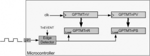
The timer can be configured to capture on the falling edge, rising edge, or both. To determine the type of edge that is captured, the TnEVENT bits of the GPTMCTL register should be initialized. See Table 8.4
Timer counting in input edge time mode
In edge time mode GPTMTnV and the optional prescaler are combined to make a 24-bit or 48-bit timer. The timer is 24-bit when 16-bit timers are used. The timer is 48-bit when 32-bit timers are used.
In up counting mode, the GPTMTnV and GPTMTnPV registers are initialized with 0s and they count up until they reach to GPTMTnILR and GPTMTnPR, respectively. Then, they are reset to 0s again.
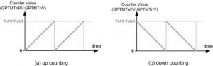
In down counting mode, the GPTMTnV and GPTMTnPV registers are initialized with GPTMTnILR and GPTMTnPR, respectively and they count down until they reach 0. Then, they are reloaded with GPTMTnILR and GPTMTnPR, again. Notice that capturing has no effect on counting and the timer continues counting when the capturing event takes place.
Initialization and Configuration for Input Edge-Time Mode
Perform the following operational steps to complete the initialization and configuration process for this mode (n = A or B):
- Disable the selected timer by clearing the TnEN bit in the GPTMCTL register.
- Initialize the GPTMCFG register by writing 0x4 to setup all timers as 16-bit default timers.
- Configure the TnMR and TnCMR fields in the GPTMTnMR register by writing:
- TnMR = 0x3 for capture mode.
- TnCMR = 0x1 for edge time mode.
- Select a count direction by programming the TnCDIR bit (0=count-down; 1=count-up).
- Configure the event type (positive-going, negative-going, or both) that the timer captures by writing the TnEVENT field of the GPTMCTL register.
- If a prescaler is to be used, write the prescale value to the GPTMTnPR register.
- Load the timer start value into the GPTMTnILR register.
- If interrupts are required, set the CnEIM bit in the GPTMIMR register.
- After these initializations and configurations are done, set the TnEN bit in the GPTMCTL register to enable the timer and begin waiting for edge events.
- If no interrupt is used, one can poll the CnERIS bit in the GPTMRIS register to wait for the edge event to occur. If interrupt is used, put appropriate codes inside the interrupt handler to process the interrupt. In both cases, the status flags are cleared by writing a 1 to the CnECIR bit on the GPTMICR register. The time at which the event happened can be obtained by reading the GPTMTnR register.
In the Input Edge Timing mode, the timer continues running after an edge event has been detected, but the timer interval can be changed at any time by writing the GPTMTnILR register and clearing the TnILD bit in the GPTMTnMR register. The change takes effect at the next cycle after the write taking placing.
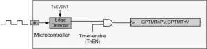
Using Timer As a Counter
As shown in Table 8.4, a timer works as a counter when the TAMR bits of the GPTMTnMR are configured to capture mode and the TACMR bit is cleared. In this situation, the timer counts whenever the input pin is triggered. See Figure 9.3. The pin can be configured to count on the falling edge, rising edge, or both. To determine the type of edge that is counted, the TnEVENT bits of the GPTMCTL register should be initialized. See Table 8.3 and Table 8.4.
Timer counting in input edge count mode
In this mode GPTMTnV and the prescaler are combined to make a 24-bit or 48-bit timer. The timer is 24-bit when TimerA and TimerB are used separately. Otherwise, they make a 48-bit timer.
In up counting mode, the GPTMTnV and GPTMTnPV registers are initialized with 0s and they count up until they reach to GPTMTnMATCHR and GPTMTnPMR, respectively. Then, they are reloaded with 0s again. See Figure 9.4.
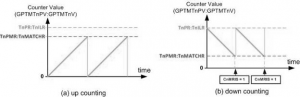
Note: The value of GPTMTnPR and GPTMTnILR must be greater than the value of GPTMTnPMR and GPTMTnMATCHR.
In down counting, the GPTMTnV and GPTMTnPV registers are initialized with GPTMTnILR and GPTMTnPR, respectively and they count down until they reach to TnMATCHR and TnPMR, respectively. Then, they are reloaded with GPTMTnILR and GPTMTnPR and the CnMRIS flag of the GPTMRIS register is set. As a result, in cases that a task must be done after a specific number of events, the registers should be initialized so that (TnPR:TnILR – TnPMR:TnMATCHR = number of events to be counted); and then the CnMRIS flag is monitored to be set.
Initialization and Configuration for Input Edge-Count Mode
Perform the following operational steps to complete the initialization and configuration process for this mode (n = A or B):
- Disable the selected timer by clearing the TnEN bit in the GPTMCTL register.
- Initialize the GPTMCFG register by writing 0x4 to setup all timers as 16-bit default timers.
- Configure the TnMR and TnCMR fields in the GPTMTnMR register by writing:
- TnMR = 0x3 for capture mode.
- TnCMR = 0x0 for edge count mode.
- Configure the event type (positive-going, negative-going or both) that the timer captures by writing the TnEVENT field of the GPTMCTL register.
- Configure the following registers according to count direction:
- In count-down mode, the GPTMTnMATCHR and GPTMTnPMR registers are configured so that the difference between the value in the GPTMTnILR and GPTMTnPR registers and the GPTMTnMATCHR and GPTMTnPMR registers equals the number of edge events that must be counted. Make sure that the value in the GPTMTnILR and GPTMTnPR registers is greater than the value in the GPTMTnMATCHR and GPTMTnPMR registers.
- In count-up mode, the timer counts from 0x0 to the value in the GPTMTnMATCHR and GPTMTnPMR registers. Note that when executing a count-up, the value of the GPTMTnPR and GPTMTnILR must be greater than the value of GPTMTnPMR and GPTMTnMATCHR registers.
- If interrupts are required, set the CnMIM bit in the GPTMIMR register.
- After these initializations and configurations done, set the TnEN bit in the GPTMCTL register to enable the timer and begin waiting for edge events.
- If no interrupt is used, one can poll the CnMRIS bit in the GPTMRIS register to wait for the edge event to be occurred. If interrupt is used, put appropriate codes inside the interrupt handler to process the interrupt. In both cases, the status flags are cleared by writing a 1 to the CnMCIR bit on the GPTMICR register.
When counting down in the Input Edge-Count Mode, the timer stops after the programmed number of edge events has been detected. To re-enable the timer, ensure that the TnEN bit is cleared and repeat steps 4 through 8.
PWM Mode
- When working in this mode, each timer can be configured as a 24- or 48-bit count-down counter to generate PWM output signals. At start, the timer loads the start values stored in the GPTMTAILR and GPTMTAPR registers (if prescaler is used) and begins its count-down actions. When gets 0, the timer reloads the start value and begin the next cycle.
- The period and frequency of the PWM signal is controlled by the start values setup in the GPTMTAILR and GPTMTAPR registers, and the pulse width is controlled by the values set in the GPTMTAMATCHR and GPTMTAPMR registers (if prescaler is used). The PWM pulse is generated (outputs High) when the timer is at its start value and terminated (outputs Low) when the timer equals to the terminate values stored in the GPTMTAMATCHR and GPTMTAPMR registers.
- The timer can generate three types of interrupt: rising edge, falling edge, and both. The event is configured by the TAEVENT field of the GPTMCTL register, and the interrupt is enabled by setting the TAPWMIE bit in the GPTMTAMR register.
- In this mode, the GPTMTAR and GPTMTAV registers always have the same value, as do the GPTMTAPS and the GPTMTAPV registers.
The operational sequence of using the Timer A to generate a PWM signal is as follows:
- The start values are loaded into the GPTMTAILR and GPTMTAPR registers, and the terminate values are loaded into the GPTMTAMATCHR and GPTMTAPMR registers. The period and duty cycle of the PWM signal are determined based on these values.
- The PWM mode is enabled with the GPTMTAMR register by setting the TAAMS bit to 1, the TACMR bit to 0, and the TAMR field to 0x2.
- The timer is enabled and starts its count-down operation by setting the TAEN bit in the GPTMCTL register to 1. The counter begins counting down until it reaches the 0 state. Then it reloads the start values and continues for the next cycle until disabled by software clearing the TAEN bit in the GPTMCTL register. Alternatively, if the TAWOT bit is set in the GPTMTAMR register, once the TAEN bit is set, the timer waits for a trigger to begin counting.
- As the timer starts counting from its start values, the PWM pulse is generated with outputting High. During the counting-down process, when the value in the timer is equal to the terminate values set in the GPTMTAMATCHR and GPTMTAPMR registers, the pulse of the PWM signal is terminated with outputting Low.
- The output level of the PWM signal can be controlled by the software, it means that the software has the capability of inverting the output PWM signal by setting the TAPWML bit in the GPTMCTL register.
Recent Comments