
GPIO – Setup the drive strength for each pin
We can setup the drive strength for each pin through the GPIODR2R, GPIODR4R, or GPIODR8R registers. This step is optional since the default drive strength is 2 mA.
The pad control registers allow software to configure the GPIO pads based on the application requirements. The pad control registers include the GPIODR2R, GPIODR4R, GPIODR8R, GPIOODR, GPIOPUR, GPIOPDR, GPIOSLR, and GPIODEN registers. These registers control drive strength, open-drain configuration, pull-up and pull-down resistors, slew-rate control and digital input enable for each GPIO. If 5 V is applied to a GPIO configured as an open-drain output, the output voltage will depend on the strength of your pull-up resistor. The GPIO pad is not electrically configured to output 5 V.
GPIO 2-mA Drive Select (GPIODR2R)
The GPIODR2R register is the 2-mA drive control register. Each GPIO signal in the port can be individually configured without affecting the other pads. When setting the DRV2 bit for a GPIO signal, the corresponding DRV4 bit in the GPIODR4R register and DRV8 bit in the GPIODR8R register are automatically cleared by hardware. By default, all GPIO pins have 2-mA drive.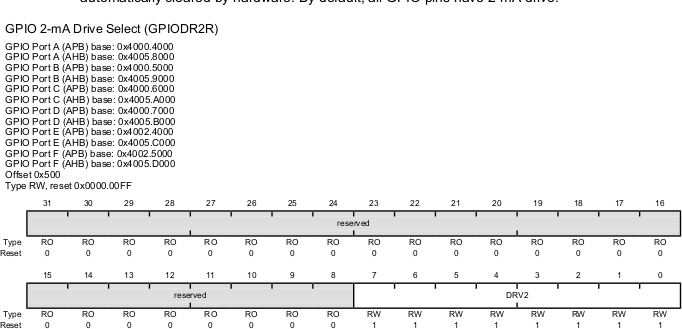
| Bit/Field | Name | Description |
|---|---|---|
| 7:0 | DRV2 | Output Pad 2-mA Drive Enable 0: The drive for the corresponding GPIO pin is controlled by the GPIODR4R or GPIODR8R register. 1: The corresponding GPIO pin has 2-mA drive. Setting a bit in either the GPIODR4 register or the GPIODR8 register clears the corresponding 2-mA enable bit. The change is effective on the second clock cycle after the write if accessing GPIO via the APB memory aperture. If using AHB access, the change is effective on the next clock cycle. |
| 31:8 | Reserved | Software should not rely on the value of a reserved bit. |
GPIO 4-mA Drive Select (GPIODR4R)
The GPIODR4R register is the 4-mA drive control register. Each GPIO signal in the port can be individually configured without affecting the other pads. When setting the DRV4 bit for a GPIO signal, the corresponding DRV2 bit in the GPIODR2R register and DRV8 bit in the GPIODR8R register are automatically cleared by hardware.

| Bit/Field | Name | Description |
|---|---|---|
| 7:0 | DRV4 | Output Pad 4-mA Drive Enable 0: The drive for the corresponding GPIO pin is controlled by the GPIODR2R or GPIODR8R register. 1: The corresponding GPIO pin has 4-mA drive. Setting a bit in either the GPIODR2 register or the GPIODR8 register clears the corresponding 4-mA enable bit. The change is effective on the second clock cycle after the write if accessing GPIO via the APB memory aperture. If using AHB access, the change is effective on the next clock cycle. |
| 31:8 | Reserved | Software should not rely on the value of a reserved bit. |
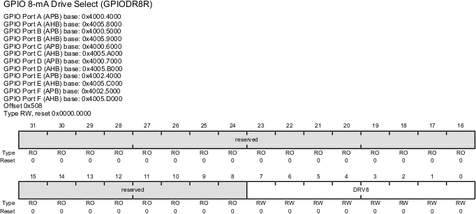
GPIO 8-mA Drive Select (GPIODR8R)
The GPIODR8R register is the 8-mA drive control register. Each GPIO signal in the port can be individually configured without affecting the other pads. When setting the DRV8 bit for a GPIO signal, the corresponding DRV2 bit in the GPIODR2R register and DRV4 bit in the GPIODR4R register are automatically cleared by hardware. The 8-mA setting is also used for high-current operation.
| Bit/Field | Name | Description |
|---|---|---|
| 7:0 | DRV8 | Output Pad 8-mA Drive Enable 0: The drive for the corresponding GPIO pin is controlled by the GPIODR2R or GPIODR4R register. 1: The corresponding GPIO pin has 8-mA drive. Setting a bit in either the GPIODR2 register or the GPIODR4 register clears the corresponding 8-mA enable bit. The change is effective on the second clock cycle after the write if accessing GPIO via the APB memory aperture. If using AHB access, the change is effective on the next clock cycle. |
| 31:8 | Reserved | Software should not rely on the value of a reserved bit.slr_r |
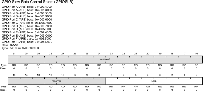
GPIO Slew Rate Control Select (GPIOSLR)
The GPIOSLR register is the slew rate control register. Slew rate control is only available when using the 8-mA drive strength option. The selection of drive strength is done through the GPIO 8-mA Drive Select (GPIODR8R) register.
| Bit/Field | Name | Description |
|---|---|---|
| 7:0 | SRL | Slew Rate Limit Enable (8-mA drive only) 0: Slew rate control is disabled for the corresponding pin.. 1: Slew rate control is enabled for the corresponding pin. |
| 31:8 | Reserved | Software should not rely on the value of a reserved bit. |
Recent Comments