
GPIO – Set up the system clock
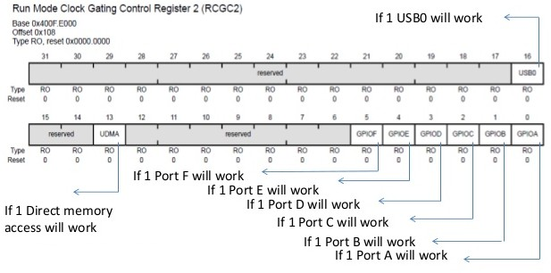
Set up the system clock for the specific GPIO Port to enable the clock to drive the port by setting the appropriate bits in the GPIO Run Mode Clock Gating Control (RCGC2) Register.
The first step to initialize the pin is to enable the clock for that port. Microcontroller disables the clock for the port to save the power and resources. For enabling the clock we deal with RCGC2 register.
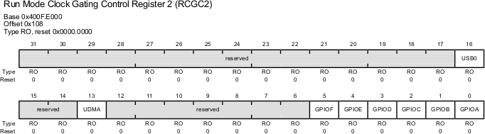
| Bit/Field | Name | Description |
|---|---|---|
| 0 | GPIOA | Port A Clock Gating Control This bit controls the clock gating for Port A. If set, the module receives a clock and functions. Otherwise, the module is unclocked and disabled. If the module is unclocked, a read or write to the module generates a bus fault. |
| 1 | GPIOB | Port B Clock Gating Control This bit controls the clock gating for Port B. If set, the module receives a clock and functions. Otherwise, the module is unclocked and disabled. If the module is unclocked, a read or write to the module generates a bus fault. |
| 2 | GPIOC | Port C Clock Gating Control This bit controls the clock gating for Port C. If set, the module receives a clock and functions. Otherwise, the module is unclocked and disabled. If the module is unclocked, a read or write to the module generates a bus fault. |
| 3 | GPIOD | Port D Clock Gating Control This bit controls the clock gating for Port D. If set, the module receives a clock and functions. Otherwise, the module is unclocked and disabled. If the module is unclocked, a read or write to the module generates a bus fault. |
| 4 | GPIOE | Port E Clock Gating Control This bit controls the clock gating for Port E. If set, the module receives a clock and functions. Otherwise, the module is unclocked and disabled. If the module is unclocked, a read or write to the module generates a bus fault. |
| 5 | GPIOF | Port F Clock Gating Control This bit controls the clock gating for Port F. If set, the module receives a clock and functions. Otherwise, the module is unclocked and disabled. If the module is unclocked, a read or write to the module generates a bus fault. |
| 12:6 | Reserved | Software should not rely on the value of a reserved bit. |
| 13 | UDMA | Micro-DMA Clock Gating Control This bit controls the clock gating for micro-DMA. If set, the module receives a clock and functions. Otherwise, the module is unclocked and disabled. If the module is unclocked, a read or write to the module generates a bus fault. |
| 15:14 | Reserved | Software should not rely on the value of a reserved bit. |
| 16 | USB0 | USB0 Clock Gating Control This bit controls the clock gating for USB module 0. If set, the module receives a clock and functions. Otherwise, the module is unclocked and disabled. If the module is unclocked, a read or write to the module generates a bus fault. |
| 31:16 | Reserved | Software should not rely on the value of a reserved bit. |
This register is 32 bit wide because of 32 bit microcontroller. For enabling the clock we deal only with the last 8 bits. Since our micro controller provides only 6 ports we are going to deal with only 6 bits from last. Writing 1 at bit 5 will enable the clock for port F.
SYSCTL_RCGC2_R |= 0x00000020; /* enable clock for PortF */
This step requires waiting for few clocks. There must be a delay of 3 system clocks after the GPIO module clock is enabled before any GPIO module registers are accessed.
Recent Comments