
SPI Protocol and DAC Interfacing
Two terminologies are widely implemented in the serial communication systems:
- Serial Communication Interface (SCI) and
- Serial Peripheral Interface (SPI).
Generally, the SCI belongs to the asynchronous serial communication interface but SPI belongs to the synchronous serial communication interface. In the TM4C123GH6PM MCU system, the SPI is used to work as a synchronous serial interface.
The fundamental difference between a UART, which implements an asynchronous protocol, and a SSI, which implements a synchronous protocol, is the manner in which the clock is implemented. Two devices communicating with asynchronous serial interfaces (UART) operate at the same frequency (baud rate) but have two separate clocks. With a UART protocol, the clock signal is not included in the interface cable between devices. Two UART devices can communicate with each other as long as the two clocks have frequencies within ±5% of each other.
Two devices communicating with synchronous serial interfaces (SSI) operate from the same clock (synchronized). With a SSI protocol, the clock signal is included in the interface cable between devices. Typically, the master device creates the clock, and the slave device(s) uses the clock to latch the data in and send data out.
Like any other serial communication interfaces, both SCI and SPI can use either full-duplex or half-duplex mode to perform the data transfers between terminals and peripherals.
The SPI (serial peripheral interface) is a bus interface incorporated in many devices such as ADC, DAC, and EEPROM. The SPI bus was originally started by Motorola (now Freescale), but in recent years has become a widely used by many semiconductor chip companies.
SPI Bus Protocol
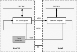
SPI devices use only 2 pins for data transfer, called SDI (Din) and SDO (Dout), instead of the 8 or more pins used in traditional buses. This reduction of data pins reduces the package size and power consumption drastically, making them ideal for many applications in which space is a major concern. The SPI bus has the SCLK (serial clock) pin to synchronize the data transfer between two chips. The last pin of the SPI bus is CE (chip enable), which is used to initiate and terminate the data transfer. These four pins, SDI, SDO, SCLK, and CE, make the SPI a 4-wire interface.
In many chips, the SDI, SDO, SCLK, and CE signals are alternatively named as MOSI (Master Out Slave In), MISO (Master In Slave Out), SCK, and SS as shown in the following Figure. There is also a widely used standard called a 3-wire interface bus. In a 3-wire interface bus, we have SCLK and CE, and only a single pin for data transfer. The SPI 4-wire bus can become a 3-wire interface when the SDI and SDO data pins are tied together. However, there are some major differences between the SPI and 3-wire devices in the data transfer protocol. For that reason, a device must support the 3-wire protocol internally in order to be used as a 3-wire device. Many devices support both SPI and 3-wire protocols.
How SPI works
SPI consists of two shift registers, one in master and the other in the slave side. Also there is a clock generator in the master side that generates the clock for the shift registers.
As you can see in the above figure, serial-out (MOSI) pin of the master shift register is connected to the serial-in (MISO) pin of the slave shift register. The master clock generator provides clock to shift register in both master and slave shift registers. The clock input of the shift registers can be falling- or rising-edge triggered.
In SPI, the shift registers are 8 bits long. It means that after 8 clock pulses, the contents of the two shift registers are interchanged. When the master wants to send a byte of data, it places the byte in its shift register and generates 8 clock pulses. After 8 clock pulses, the byte is transmitted to the slave shift register. When the master wants to receive a byte of data, the slave side should place the byte in its shift register and after 8 clock pulses the data will be received by the master shift register. It must be noted that SPI is full duplex meaning that it sends and receives data at the same time.
Clock polarity and phase in SPI device
In UART communication, transmitter and receiver must agree on a clock frequency (baud rate). In SPI communication, both master and slave uses the same clock but the master and slave(s) must agree on the clock polarity and phase with respect to the data. Freescale names these two options as CPOL (clock polarity) and CPHA (clock phase) respectively. At CPOL=0 the idle value of the clock is zero while at CPOL=1 the idle value of the clock is one.
- CPHA=0 means sample data on the leading (first) clock edge, while
- CPHA=1 means sample data on the trailing (second) clock edge.
Notice that if the idle value of the clock is zero the leading (first) clock edge is a rising edge but if the idle value of the clock is one, the leading (first) clock edge is a falling edge.
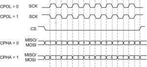
| CPOL | CPHA | Data Read and Change Time | SPI Mode |
|---|---|---|---|
| 0 | 0 | read on rising edge, changed on a falling edge | 0 |
| 0 | 1 | read on falling edge, changed on a rising edge | 1 |
| 1 | 0 | read on falling edge, changed on a rising edge | 2 |
| 1 | 1 | read on rising edge, changed on a falling edge | 3 |
Recent Comments