
GPIO Port Interrupt Programming
Interrupt numbers 16 to 255 are assigned to the peripherals. The INT (IRQ) 46 is assigned to the GPIO Port of F. Although PortF has 8 pins, we have only one interrupt assigned to the entire PortF. In other words, when any of the PortF pins trigger an interrupt, they all go to the same address location in the interrupt vector table. It is the job of our Interrupt Service Routine (ISR or interrupt Handler) to find out which pin caused the interrupt.
Interrupt trigger point
When an input pin is connected to an external device to be used for interrupt, we have 5 choices for trigger point. They are:
- low-level trigger (active Low level),
- high-level trigger (active High level),
- rising-edge trigger (positive-edge going from Low to High),
- falling-Edge trigger (negative-edge going from High to Low),
- Both edge (rising and falling) trigger.
Upon Reset, all the interrupts are disabled. To enable any interrupt:
- Enable the interrupt for a specific peripheral module.
- Enable the interrupts at the NVIC module.
- Enable the interrupt globally
GPIO Interrupt Control Registers
| GPIO Register | Tivaware Name | Each Bit Value (Lowest 8-Bit) and Each Pin Function |
|---|---|---|
| GPIOIS | GPIO_PORTx_IS_R | Interrupt sense register Determines level or edge triggered 0: Detect an edge (edge-sensitive) on the pin, 1: Detect a level (level-sensitive) on the pin. |
| GPIOIBE | GPIO_PORTx_IBE_R | 0: Interrupt is controlled by GPIOIEV, 1: Both edges on the corresponding pin trigger an interrupt |
| GPIOIEV | GPIO_PORTx_IEV_R | GPIO Interrupt Event Register Determines the detecting edges or levels. 0: A falling edge or a LOW level, 1: A rising edge or a HIGH level triggers an interrupt |
| GPIOIM | GPIO_PORTx_IM_R | GPIO Interrupt Mask Register Masks (disables) or unmask (enable) an interrupt. 0: Interrupt is masked (disabled), 1: Interrupt is unmasked (enabled). |
| GPIORIS | GPIO_PORTx_IS_R | GPIO Raw Interrupt Status Register Indicates the raw interrupt status for a pin. 0: No interrupt occurred on the pin, 1: An interrupt is occurred on the pin. For the edge-triggered interrupts, write a 1 to the pin to clear that interrupt. For level-triggered interrupt, no action is needed. |
| GPIOMIS | GPIO_PORTx_MIS_R | GPIO Masked Interrupt Status Register Indicates the state of the interrupt. 0: No interrupt occurred or the pin has been masked, 1: An interrupt has been occurred. |
| GPIOICR | GPIO_PORTx_ICR_R | GPIO Interrupt Clear Register Clears an edge-triggered interrupt. 0: No action, 1: The corresponded edge-triggered interrupt is cleared. |
- All of these registers are 32-bit, but only lowest 8 bits are used and each bit corresponds to each pin in the selected GPIO Port: bit 0 is for pin 0, bit 1 is for pin 1, and so on. The above table shows the bit values and their functions for these registers.
- Before any exception or interrupt can be applied to any pin on any GPIO Port, all GPIO pins on selected GPIO Port should be initialized and configured via related GPIO registers.
GPIO Interrupt Control Registers Description
GPIO Interrupt sense register (GPIOIS)

| Bit | Bit Name | Description |
|---|---|---|
| 7-0 | IS | GPIO Interrupt Sense 0: The edge on the corresponding pin is detected (edge-sensitive). 1: The level on the corresponding pin is detected (level-sensitive). |
First, we must use GPIO Interrupt Sense (GPIOIS) register to decide the level or edge. Only after using the GPIOIS register we need to indicate which level or edge. To do that, we use the GPIO Interrupt Event (GPIOIEV) to decide low-level, high-level, falling, or rising-edge. The GPIO Interrupt Both Edges (GPIOIBE) register bits overwrite the decision in GPIOIEV. Unless both edge interrupt is desired, the bit in GPIOIBE needs to be cleared.
GPIO Interrupt Event Register (GPIOIEV)
| GPIOIS (interrupt sense) |
GPIOIEV (Interrupt Event) |
|
|---|---|---|
| 0 | 0 | Falling edge |
| 0 | 1 | Rising edge |
| 1 | 0 | Low level |
| 1 | 1 | High level |
- Since we need a rising edge triggered interrupt at PF4, so writing 1 to the respective bit field will do the same for us.
GPIO Interrupt Both Edge (GPIOIBE)
| Bit | Bit Name | Description |
|---|---|---|
| 7-0 | IBE | GPIO Interrupt Both Edges 0: Interrupt generation is controlled by the GPIO Interrupt Event (GPIOIEV) register 1: Both edges on the corresponding pin trigger an interrupt |
- Setting the corresponding bit field enables the interrupts for both edges i.e. rising edge and falling edge but our concern is to enable the interrupts for rising edge only. Making the corresponding bit field i.e. PF4 to 0 will allow us to use this register in conjunction with the GPIOIEV register.
GPIO Interrupt Clear Register (GPIOICR)
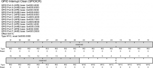
- The corresponding bit fields in this register clears the interrupt for the respective pin. To ensure that any previous interrupt has been cleared writing 1 to the respective bit field will clear the interrupt on that pin.
- It is critical that the interrupt handler clears the interrupt flag before returning from interrupt handler. Otherwise the interrupt appears as if it is still pending and the interrupt handler will be executed again and again forever and the program hangs.
GPIO Interrupt Mask Register (GPIOIM)
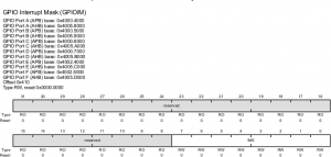
- We need to enable the interrupt capability of a given peripheral at the module level. This should be done after other configurations of that peripheral are done. In the case of I/O ports, each pin can be used as a source of external hardware interrupt. This is done with the GPIO Interrupt Mask (GPIOIM) register.
- Notice that, the lower 8 bits of this register is used to enable the interrupt capability of each pin of the I/O port. To enable the interrupts for PF0 and PF4 pins, we will need the following:
GPIO_PORTF_IM_R |= 0x11; /* unmask interrupt */
GPIO Raw Interrupt Status (GPIORIS)
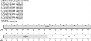
| Bit | Bit Name | Description |
|---|---|---|
| 7-0 | RIS | GPIO Interrupt Raw Status 0: An interrupt condition has not occurred on the corresponding pin. 1: An interrupt condition has occurred on the corresponding pin. |
- For edge-detect interrupts, this bit is cleared by writing a 1 to the corresponding bit in the GPIOICR register.
- For a GPIO level-detect interrupt, the bit is cleared when the level is deasserted.
GPIO Masked Interrupt Status (GPIOMIS)
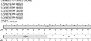
| Bit | Bit Name | Description |
|---|---|---|
| 7-0 | MIS | GPIO Masked Interrupt Status 0: An interrupt condition on the corresponding pin is masked or has not occurred. 1: An interrupt condition on the corresponding pin has triggered an interrupt to the interrupt controller. |
- For edge-detect interrupts, this bit is cleared by writing a 1 to the corresponding bit in the GPIOICR register.
- For a GPIO level-detect interrupt, the bit is cleared when the level is deasserted.
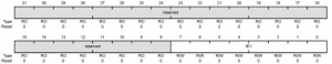
NVIC Interrupt Priority Register
| Bit/Field | Name | Description |
|---|---|---|
| 7:5 | INTA | Interrupt Priority for Interrupt [4n] This field holds a priority value, 0-7, for the interrupt with the number [4n], where n is the number of the Interrupt Priority register (n=0 for PRI0, and so on). The lower the value, the greater the priority of the corresponding interrupt. |
| 15:13 | INTB | Interrupt Priority for Interrupt [4n+1] This field holds a priority value, 0-7, for the interrupt with the number [4n+1], where n is the number of the Interrupt Priority register (n=0 for PRI0, and so on). The lower the value, the greater the priority of the corresponding interrupt. |
| 23:21 | INTC | Interrupt Priority for Interrupt [4n+2] This field holds a priority value, 0-7, for the interrupt with the number [4n+2], where n is the number of the Interrupt Priority register (n=0 for PRI0, and so on). The lower the value, the greater the priority of the corresponding interrupt. |
| 31:29 | INTD | Interrupt Priority for Interrupt [4n+3] This field holds a priority value, 0-7, for the interrupt with the number [4n+3], where n is the number of the Interrupt Priority register (n=0 for PRI0, and so on). The lower the value, the greater the priority of the corresponding interrupt. |
| PRIn Register Bit Field | Interrupt Source | Priority Register Macros |
|---|---|---|
| Bits 31:29 | Interrupt[IRQ] = Interrupt[4n+3] | NVIC_PRIn_R |
| Bits 23:21 | Interrupt[IRQ] = Interrupt[4n+2] | |
| Bits 15:13 | Interrupt[IRQ] = Interrupt[4n+1] | |
| Bits 7:5 | Interrupt[IRQ] = Interrupt[4n] |
- Table 7.5 represents the priority register bit fields against the interrupt sources. This priority register bit field is 3-bits wide which means that for an interrupt there can be eight priority levels from 000 to 111 and it can be programmed as per the need.
- n represents the group number of priority registers, for each group n registers NVIC_PRIn can control up to 4 peripheral ranging from 4n to 4n+3.
- To understand this better just take an example, suppose that for an interrupt handler whose IRQ number is 0, in order to satisfy the equation interrupt[4n]=0 the value of n must be zero which corresponds to the NVIC_PRI0_R also this same register can configure the priority levels for 4n to 4n+3 peripherals.
- In this case the value of n is 0 therefore the same priority level register can be used to configure the interrupts whose IRQ Number are within 4×0 to 4×0+3, which corresponds to the IRQ number 0,1,2,3.
- In tm4c123gh6pm_startup_ccs_gcc.c file the IRQ number 0 to 3 represents the interrupt handlers for GPIOA to GPIOD respectively. In a program for each interrupt the priority level can be set in the corresponding bit fields.
Table 7.6 shows some of the priority registers on the NVIC. Each register contains an 8-bit priority field for four devices. On the TM4C micro controllers, only the top three bits of the 8-bit field are used. This allows us to specify the interrupt priority level for each device from 0 to 7, with 0 being the highest priority.
| Address | 31 – 29 | 23 – 21 | 15 – 13 | 7 – 5 | Name |
|---|---|---|---|---|---|
| 0xE000E400 | GPIO Port D | GPIO Port C | GPIO Port B | GPIO Port A | NVIC_PRI0_R |
| 0xE000E404 | SSI0, Rx Tx | UART1, Rx Tx | UART0, Rx Tx | GPIO Port E | NVIC_PRI1_R |
| 0xE000E408 | PWM Gen 1 | PWM Gen 0 | PWM Fault | I2C0 | NVIC_PRI2_R |
| 0xE000E40C | ADC Seq 1 | ADC Seq 0 | Quad Encoder 0 | PWM0 Gen 2 | NVIC_PRI3_R |
| 0xE000E410 | Timer 0A | Watchdog | ADC Seq 3 | ADC Seq 2 | NVIC_PRI4_R |
| 0xE000E414 | Timer 2A | Timer 1B | Timer 1A | Timer 0B | NVIC_PRI5_R |
| 0xE000E418 | Comp 2 | Comp 1 | Comp 0 | Timer 2B | NVIC_PRI6_R |
| 0xE000E41C | GPIO Port G | GPIO Port F | Flash Control | System Control | NVIC_PRI7_R |
| 0xE000E420 | Timer 3A | SSI1, Rx Tx | UART2, Rx Tx | GPIO Port H | NVIC_PRI8_R |
| 0xE000E424 | CAN0 | Quad Encoder 1 | I2C1 | Timer 3B | NVIC_PRI9_R |
| 0xE000E428 | Hibernate | Ethernet | CAN2 | CAN1 | NVIC_PRI10_R |
| 0xE000E42C | uDMA Error | uDMA Soft Tfr | PWM Gen 3 | USB0 | NVIC_PRI11_R |
| 0xE000ED20 | SysTick | PendSV | — | Debug | NVIC_SYS_PRI3_R |
- The interrupt number is loaded into the IPSR register. The servicing of interrupts does not set the I bit in the PRIMASK, so a higher priority interrupt can suspend the execution of a lower priority ISR.
- If a request of equal or lower priority is generated while an ISR is being executed, that request is postponed until the ISR is completed. In particular, those devices that need prompt service should be given high priority.
Enabling and Disabling an Interrupt
Upon Reset, all the interrupts are disabled. To enable any interrupt we should:
- Enable the interrupt for a specific peripheral module.
- This is done with the GPIO Interrupt Mask (GPIOIM) register.
- Enable the interrupts at the NVIC module.
- Enable the interrupt globally .
Interrupt enabling with all 3 levels
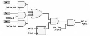
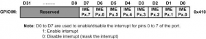
Figure:GPIO Interrupt Mask (GPIOIM)
Interrupt Set Enable Register
It is the interrupt set enable register ranging from NVIC_EN0_R … NVIC_EN3_R, each ISER register is 32 bit wide that can be used to set the interrupt against the respective IRQ numbers. Each ISER register can be used to enable 32 different types of interrupt sources. For example NVIC_EN0_R is used to enable the interrupt sources whose IRQ numbers are 0-31, similarly the interrupt sources whose IRQ numbers are 32-63 can be enabled by NVIC_EN1_R and so on. The corresponding bit field is required to be set according to the IRQ number of the interrupt sources since each register is 32 bit wide. If the interrupt source whose IRQ number is greater than 31 the corresponding bit number can be calculated by this formula:
bit number = IRQ number - 32(n-1)
where n=1 for interrupt sources having IRQ number 0-31. Similarly n=2 for interrupt sources having IRQ number 32-63 and so on. For enabling interrupt at PF4 pin writing 1 to the bit field 30 of NVIC_EN0_R will do the same for us, as its IRQ number is 30.
To disable interrupts there are another registers: NVIC_DIS0_R to NVIC_DIS3_R (Interrupt Clear Enable). Writing zeros to the NVIC_EN0_R through NVIC_EN3_R registers has no effect. To disable interrupts we write ones to the corresponding bit in the NVIC_DIS0_R through NVIC_DIS3_R register.
| Enable Register | 32-Enable Bits | Address | ||||||||
|---|---|---|---|---|---|---|---|---|---|---|
| 0 | 1 | 2 | 3 | 4 | 5 | 6-29 | 30 | 31 | ||
| NVIC_EN0_R | PORTA | PORTB | PORTC | PORTD | PORTE | UART0 | … | PORTF | PORTG | 0xE000E100 |
| NVIC_EN1_R | PORTH | UART2 | SSI1 | Timer3A | Timer3B | I2C1 | … | UART6 | UART7 | 0xE000E104 |
| NVIC_EN2_R | … | … | … | … | I2C2 | I2C3 | … | WTimer0A | WTimer0B | 0xE000E108 |
| NVIC_EN3_R | WT1A | WT1B | WT2A | WT2B | WT3A | WT3B | … | GPIOQ2 | GPIOQ3 | 0xE000E10C |
Global interrupt enable/disable
Global interrupt enable/disable allows us with a single instruction to mask all interrupts during the execution of some critical task such as manipulating a common pointer shared by multiple threads. In ARM Cortex M, we do the global enable/disable of interrupts with assembly language instructions of CPSID I (Change processor state-disable interrupts) and CPSIE I (Change processor state-enable interrupts). In C language we use inline assembly language instructions:
void DisableInterrupts(void){__asm ("CPSID  I\n");}
void EnableInterrupts(void){__asm  ("CPSIE  I\n");}
Initialize and Configure GPIO Interrupt Control Registers
To initialize and configure GPIO interrupt controls, one needs to program the GPIOIS, GPIOIBE, GPIOEV, and GPIOIM registers to configure the type, event, and mask of the interrupts for each port. The following steps should be used to do this initialization and configuration process:
- Configure the GPIOIM register to disable (mask) the undesired pins.
- Configure the GPIOIS register to indicate the interrupt-triggering type, edge, or level.
- Configure the GPIOIBE register to indicate if this interrupt is triggered by both edges.
- Reset the GPIORIS register to 0 to make it ready to set a flag if any interrupt occurred.
- Configure the GPIOIM register to enable (unmask) the desired pins.
How to configure and set up an interrupt and its handler
Now let’s provide an example to illustrate how to configure and set up an interrupt and its handler based on the above Tables. For example, we want to set up and configure an interrupt for GPIO PortF. Perform the following operations to complete this job:
- Find the IRQ number for this interrupt from Table 7.3. The IRQ number for the GPIO PortF is 30.
- Based on Table 7.6, obtain the group number of the priority register (n). The IRQ number is 30. In order to make the equation 30 = interrupt[4n + 2] hold, n must be 7. This means that we need to use group 7 priority register NVIC_PRI7_R with bits 23-21 to configure the priority level for the GPIO PortF. Since the IRQ number of this port is 30, we can set the priority level for this port as 5, (101B), in bits 23-21 on the NVIC_PRI7_R. This setup can be written as NVIC_PRI7_R = (NVIC_PRI7_R & 0xFF00FFFF) | 0x00A00000 in the user’s program.
- Based on Table 7.7, obtain the bit field in the NVIC Set Enable Register to enable this port. Since the IRQ number of the Port F is 30, the bit 30 in the NVIC_EN0_R register should be set to 1 to enable this port. This setup can be written as NVIC_EN0_R = 0x40000000.
- Open tm4c123gh6pm_startup_ccs_gcc.c for editing. This file contains the vector table among other things. Open the file and look for the GPIO PortF vector. You need to carefully find the appropriate vector position and replace IntDefaultHandler with the name of your Interrupt handler.
- After going through all these steps an EnableInterrupts() function is called to perform the global interrupt enable function. Note that we have to enable the pull up at PF4 in order to provide high or low input signal.
- It is critical that the interrupt handler clears the interrupt flag before returning from interrupt handler. Otherwise the interrupt appears as if it is still pending and the interrupt handler will be executed again and again forever and the program hangs. The PORTF interrupt flag is cleared by writing a 1 to the bit that corresponds to the pin that triggered the interrupt in the GPIO Interrupt Clear Register (GPIOICR). In the case of SW1 (PF4), the interrupt flag is cleared by:
GPIO_PORTF_ICR_R = 0x10;
Note:The ARM Cortex writes are buffered. That means a write does not take effect immediately. It may take many clock cycles before the write to ICR to clear the interrupt flags. When return from interrupt handler and the interrupt flag is still pending, the interrupt handler will be executed again. One way to ensure that interrupt flags are cleared before returning from interrupt handler is to perform a read to force the write to take effect.
Recent Comments