
This page describes the Signal Generator using DAC and DMA on STM32L Discovery Board Project, which is a part of the Embedded Systems-1 course. The aim of this project is to develop a signal generator capable of generating sine, triangular and square waves using STM32L Discovery Board with the help of on board peripherals such as DAC,DMA,GPIO, Timer etc.A schematic of STM32L Discovery Board is included for reference.
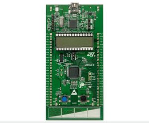
STM32L Discovery Board
Overview
The basic approach was to use Lookup tables for the different waves and transfer them via DMA from memory to the DAC (which inturn is triggered by timers) which gives an analog output which can be viewed on a DSO.Using DMA helps in transferring samples at high frequency and all the while the core remains free and available for other tasks.The variable frequency was achieved by varying the time interval between samples.The User button onboard STM2l Discovery was used to vary the frequency of different waves and an external button(interfaced as an interrupt source via GPIO) was used to switch between the different waves.
Block Diagram
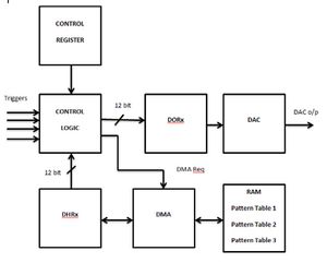
Block Diagram
Hardware Configuration and Detailed Working
DAC
- 12 bit right aligned mode used and hence the address of the data holding register DHR12Rx, 0x40007414 is given as the peripheral destination address for the DMA.
- Because the DAC has unsigned resolution an offset has to be added to the samples while creating the lookup table so that minimum value is 0.
- DAC channel 2 was configured to be used with Timer 2 as the trigger (external trigger) and hence everytime a Timer 2 trigger occurs the values in the DHR register is transfered to the corresponding DOR register and the analog output is available after a T_settling(conversion time) at the output pin PA4(PA5 in case of DAC channel 1).
- Trigger events can include the trigger signals from various timers (TIM2-TIM7, TIM15), an external interrupt (EXTI line 9), and software. It is also possible to configure the DAC without a trigger in which case DHRx is automatically copied to the DORx after a single clock cycle delay.
Using DAC with DMA
- STM32L Microcontrollers DAC channel 1 is connected to the DMA channel 2 and DAC channel2 is connected to DMA channel 3 [Reference Manual].
- When DAC-DMA is enabled, everytime the timer triggers a DMA request is generated which transfers the data from DMA source(Lookup table in memory) to DMA destination(corresponding DHR register) and the trigger also initiates the transfer of data from DHR to DOR and hence the DAC conversion process.
- It must be noted that in the case of an external trigger the transfer from DHR to DOR takes place atleast 3 clock cycles after the trigger occurs and the conversion takes T_settling amount of time.Hence the timer must be configured such that this minimum interval is kept between triggers otherwise it may lead to distorted waves owing to missing samples.
The DAC channel 2 and hence the DMA channel 3 were chosen for use in this project and the output waveform was observed by connecting the DSO probe to PA5.
DAC Output Voltage
Digital inputs are converted to output voltages on a linear conversion between 0 and VREF+. The analog output voltages on each DAC channel pin are determined by the following equation:
Vout                  =            DAC_DORx value * Vref
	                           ---------------------	Vref =Vdd for the board
			                 4095
Waveform Frequency
The frequency of the waveform is calculated by the eqn:
Output frequency      =	             System clock frequency
			       -----------------------------------------------
			       No: of samples * Clock Period * Prescaler Value
Hence the prescaler and period must be adjusted such that the gap of 3-4 APB cycles + settling time is adequately available between each trigger. This is the basic limiting factor in achieving maximum frequency.Another limiting factor is that the maximum frequency for all the peripherals is 32Mhz.
Clock Configuration
- To ensure higher frequency of operation,the PLL was configured to operate at 24 MHz using internal HSI oscillator (16 MHz) as the entry clock.
- PLL was then used as the system clock source and the AHB,APB1 and APB2 clocks are also configured to operate at same 24 MHz.
Timer Configuration
- Timer 2 was configured in up counting mode, where the counter counts from 0 to the auto-reload value (content of the TIMx_ARR register), then restarts from 0 and generates a counter overflow event.
- The timer has two basic parameters – Period and Prescaler.
- Period decides till which count we go upto before we generate the trigger and restart counting.Prescaler decides once in how many clock cycles the count value gets updated.
- The good thing about these two parameters is that both can be varied on the fly .ie. once updated they change automatically from the next cycle and no deinit and re-initialization is required to change them.This helps to easily update the frequency of the waves. Each press on the user button loads the prescale register with a new value corresponding to the new frequency.
User Button
- The user button (PA.0) was configured as External interrupt Line 0.
- The corresponding interrupt handler takes care of the switching between different frequencies on each user button press by changing the prescaler value to be loaded into the prescale register of the timer.
- The priority of the interrupt is appropriately set ( low priority as compared to external push button interrupt) and is configured to trigger on the rising edge.
External Push Button
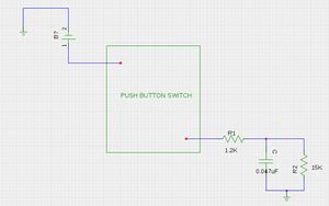
Debouncing Circuit for external Push Button
- An external push button with associated debouncing circuitry was used to switch between waveforms.
- GPIO pin PC.1 was configured as input and also set as the source for the External interrupt Line 1.
- Configured to be triggered on the rising edge with a priority value higher than that of the userbutton interrupt by changing the subpriority.
- The corresponding interrupt handler takes care of the switching between waveforms by first disabling the DAC and its DMA, loading the source memory address with the new set of values corresponding to the new waveforms, followed by enabling the DAC and DMA again.
- A debouncing circuitry was set up so as to prevent the push button from generating multiple pulses which may generate multiple interrupts on a single key press.
Low Power Mode
- Sleep mode was chosen since in this mode the core is entirely stopped but all the peripherals are up and running.Also no other clocks are affected.
- Whenever an interrupt occurs,core wakes up, excecutes the corresponding handler function and again goes back to Sleep.
- Debug support is also provided in low power mode to aid debugging.
External Connections to the Board
| Source | Destination | Purpose | |
| 1. | One pin of push button | Vdd on board | To provide a rising edge to PC.1 on each button press |
| 2. | Pair pin of push button | PC.1 | To configure PC.1 as external interrupt activated on the button press |
| 3. | One end of 15 K and 0.047uF capacitor | GND on board | Connection to the GND completes the loop |
| 4. | DSO probe | PA.5 | To view the waveform on DSO |
Key Points to Remember
- DAC channels 1 and 2 are connected to DMA channel 2 and 3 respectively. Many documents were found to wrongly cite this information as DAC channels 1 and 2 being connected to DMA channels 3 and 4 respectively.
- It is better to use DAC channel 2 for a proper output. It was found that DAC Channel 1 gives a lower frequency for the same configuration as channel 2.
Software Algorithm and Flowchart
Pseudo Code
1.CLOCK configuration.
2.INITIALIZATIONS – Dac, Dma, Timer,Gpio.
3.DAC-DMA enabled -> Wave Generation begins.
4.Enter SLEEP mode.
5.WAKE UP on interrupt and excecute corresponding handler and back to step 4.
Flow Chart
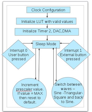
Flow Chart
Source Code
The source code can be found at moodle.
Team Members
- Prathyusha G
- Swathy Sen
Recent Comments