
This page describes the project Signal Generator using STM32LDiscovery Board, which is a part of Embedded Systems-I course. The aim of the project is to generate sine, triangle and square waves using built in timer, DAC and DMA.
STM32L Discovery Board
Introduction
The look up tables for various waves are stored in memory. The number of samples are dynamically decided according to the frequency selected by the user. The timer is used to decide the time between two successive samples. When the timer overflows, it triggers the DAC to generate a DMA request which transfers the next sample. Thus the required wave is generated. The user button is used to toggle between the different waves and also the frequency range required(Low, Medium and High). The Touch Screen is used to vary the frequency of the corresponding wave.
Block Diagram
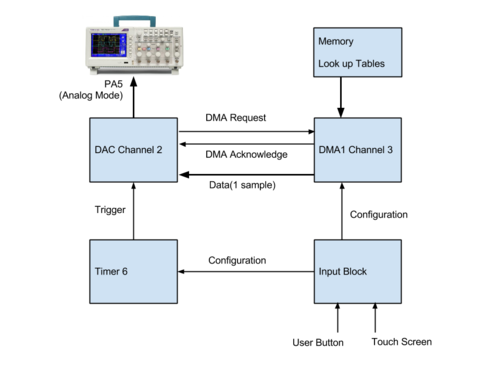
Block Diagram
Configuration
DAC Configuration
- 12 bit right aligned mode
- Output Buffers Enabled
- Trigger Source: Timer 6 update event
- Enable DMA Request Generation when trigger received from timer.
DMA Configuration
- In STM32L152 microcontroller DAC Channel 2 connected to DMA1 Channel 3.
- DMA Mode : Circular
- DMA Buffer Size : 25 to 280
- DMA Transfer Direction : Peripheral as a destination
- DMA Memory to Memory Transfer was disabled.
- DMA Memory Base Addr : base address of look up table which is changed dynamically;
- DMA Memory and Peripheral Data Size : Half word (16 bits)
- DMA Memory Increment : Enable
- DMA Peripheral Base Addr : Address of DHR register
- Disable Peripheral Increment as we are writing at the same location.
Timer Configuration
- Counter Mode: up counter
- The period and prescaler are set dynamically according to the user button and touch screen slider position.
Calculations
DAC Output Voltage
The analog output voltage can be calculate by following equation:
                    DAC_DORx value * Vref
Vout       =        ---------------------	(Vref = Vdd for the board)
			     4095
The frequency of output waveform can be calculate by following equation:
	                                               Peripherals clock frequency
Output waveform frequency      =     ------------------------------------------------------------------
			                No. of samples in one cycle * Clock Period * Prescaler Value
- Theoretically, maximum frequency can be achieved by providing the maximum 32 MHz clock to the timer using PLL, setting prescaler to 0 and ARR to 1. However, beyond ARR=16 waves were getting distorted.
- This gives minimum time between samples as
             16
     ------------------- = 500 ns
       (32 × (10)^6 )
- For minimum 25 samples, maximum achievable frequency is 1/(25×500) GHz=80KHz
- However practically, a maximum of 76 KHz was achievable without wave distortion.
Problems faced
- When we used DAC_Channel1, the maximum frequency we could achieve was 1 KHz. However we could get a maximum of 76 KHz using DAC_Channel2. Thus, the current sourcing capability of DAC2 is more than that in DAC1.
- Enable the output buffers of the DAC to provide more current sourcing capability.
- In STM32LDiscovery Demo Project the DAC and the corresponding DMA are incorrectly mapped. DAC1 is connected to DMA Channel2 whereas DAC2 is connected to DMA Channel3.
- Once initialized, the DMA parameters do not change by directly changing the register. You have to de-initialize and re-initialize the DMA for the changes to be effective.
References
- RM0038 Reference manual STM32L151xx, STM32L152xx and STM32L162xx advanced ARM-based 32-bit MCUs
- UM1079 User manual STM32L-DISCOVERY
- stm32l-discovery-schematic
Team Members
- Anuj Jain(anuj.jain@dese.iisc.ernet.in)
- Piyush Patel(piyush@cedt.iisc.ernet.in)
Recent Comments