
Programming PWM in TI Tiva LaunchPad
PWM Clock source
The Clock source to the PWM module in TI Tiva LaunchPad is enabled via R1 or R0 bits of RCGCPWM register. The RCGCPWM register is part of the System Control registers and located at the physical address of 0x400F.E000 with offset 0x640. See Figure 15.21.
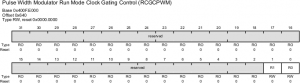
We enable the clock source to PWM0 module with SYSCTL_RCGCPWM_R |= 1; and to PWM1 module with SYSCTL_RCGCPWM_R |= 2;
SYSCTL_RCGCPWM_R |= 1;  /* enable clock source to PWM0 module */
SYSCTL_RCGCPWM_R |= 2;  /* enable clock source to PWM1 module */
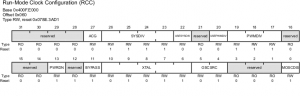
Run-Mode Clock Configuration (RCC)
This register is used to pre-divide the system clock before feeding it to the PWM modules. The clock source to the PWM module may come directly from the system clock or after going through a divider. See Figures 15.22 and 15.23.
| bit | Name | Description | ||||||||||||||||||
|---|---|---|---|---|---|---|---|---|---|---|---|---|---|---|---|---|---|---|---|---|
| 19-17 | PWMDIV | PWM Unit Clock: The System Clock is divided by 2PWMDIV-1 when the USEPWMDIV bit is set one.
|
||||||||||||||||||
| 20 | USEPWMDIV | Enable PWM Clock Divisor (Use PWM clock Divisor) 0: The PWM clock divider is by passed. 1: The PWM clock divider is used as the PWM clock source. |
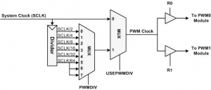
The D20 bit (USEPWMDIV) of RCC register allows us to make this selection. With Bit D20 = 1, we have the choices of dividing the system clock by 2, 4, 8, 16, 32, and 64 (default) before it is fed to the PWM modules. The D19-D17 bits of RCC register determines the value of the divisor. Notice that the default is divide by 64 if the pre-divider is enabled by D20 bit.
Example:
Find the value of bit 20-17(PWMDIV) of the RCC register for PWM Module clock frequencies of (a) 8MHz, (b) 2MHz, (c) 1MHz, and (d) 250KHz. Assume the system clock frequency is 16MHz.
Solution:
With D20 = 1, we have the following:
(a) D19-D17 = 000 gives us 16MHz/2=8MHz for PWM Module Frequency.
(b) D19-D17 = 010 gives us 16MHz/8=2MHz for PWM Module Frequency.
(c) D19-D17 = 011 gives us 16MHz/16=1MHz for PWM Module Frequency.
(d) D19-D17 = 111 gives us 16MHz/64=250KHz for PWM Module Frequency (default).
Enabling PWMx Generator (Counter)
In TI Tiva LaunchPad, we have two PWM modules PWM0 and PWM1. Each PWM module has four Generators (Counters) as shown in Figure 14.1. Figure 15.24 shows the simplified structure of a Generator.
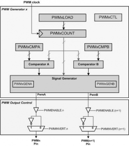
We use PWMxCTL (PWMx Control) register to enable the Generator (Counter). Notice that we use the terms Counter and Generator interchangeably since there is one Counter per Generator and all the programming of the Generator surrounds the Counter. Also notice that we have a PWMxCTL for each Generator. See Figure 15.25.
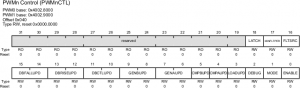
The most important bit of the PWMxCTL is D0 (Enable). This bit is used to start or stop the Counter. The next important bit is D1 (MODE). The counter has two modes:
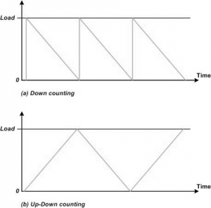
- Count Down: counts down from the load value until it reaches 0. Upon reaching zero, the load value is placed in the counter and the countdown starts again. This is the default option.
- Count Up-Down: counts up from 0 until it reaches the load value. After reaching the load value, it turns around and counts down to 0 and upon reaching 0 it repeats the process. See Figure 15-26.
In both modes, the load value is in a register called LOAD (PWMxLOAD) register. Notice that we must disable a given Generator (Counter) before the initialization. After the initialization is done, we must enable it to start counting.
Table 15-21 shows the offset address for Control register of PWM0 Module. We also have four Control registers for PWM1 Module. The offset addresses are the same except the Base address for the PWM1 module is different, as we mentioned earlier.
| Register | Offset |
|---|---|
| PWM0_0_CTL (Control for Counter0) | 0x040 |
| PWM0_1_CTL (Control for Counter1) | 0x080 |
| PWM0_2_CTL (Control for Counter2) | 0x0C0 |
| PWM0_3_CTL (Control for Counter3) | 0x100 |
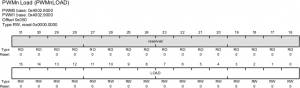
The LOAD register
To set the maximum value for the Counter, we have to load register called PWMxLOAD. Since each of PWM0 and PWM1 has four Generators (Counters), we also have four PWMxLOAD registers. The PWMxLOAD register is 16-bit wide and it determines the maximum count and hence the PWM output frequency.
Figure 15.27 shows the LOAD registers of PWM0 Module. We also have four LOAD registers for PWM1 Module. The offset addresses are the same except the base address for the PWM1 module is different, as we mentioned earlier.
| Register | Offset |
|---|---|
| PWM0_0_LOAD | 0x050 |
| PWM0_1_LOAD | 0x090 |
| PWM0_2_LOAD | 0x0D0 |
| PWM0_3_LOAD | 0x110 |
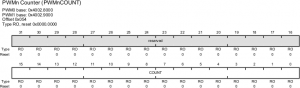
Reading the Current Counter Value
The current value of the Counter (Generator) can be read from the PWMxCOUNT register. As the Counter (Generator) counts up or counts down, we can read the value of this register at any time. Notice, this is a Read-Only (RO) register. Since the Counter is 16-bit, the PWMxCOUNT gives us the current value of the counter which can be between 0 to 0xFFFF. We can set a maximum value for the Counter using the LOAD register. Figure 15.28 shows the Current Count registers of PWMn Module.
| Register | Offset |
|---|---|
| PWM0_0_COUNT | 0x054 |
| PWM0_1_COUNT | 0x094 |
| PWM0_2_COUNT | 0x0D4 |
| PWM0_3_COUNT | 0x114 |
We also have four Current Count registers for PWM1 Module. The offset addresses are the same except the Base address for the PWM1 module is different, as we mentioned earlier.
Compare A and Compare B
Figure 15-29 shows the offset addresses for CompareA registers of PWM0 Module. We also have four CompareA registers for PWM1 Module. The offset addresses are the same except the Base address for the PWM1 module is different, as we mentioned earlier.
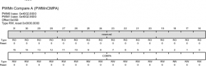
| Register | Offset |
|---|---|
| PWM0_0_CMPA | 0x058 |
| PWM0_1_CMPA | 0x098 |
| PWM0_2_CMPA | 0x0D8 |
| PWM0_3_CMPA | 0x118 |
Figure 15-30 shows the offset addresses for CompareB registers of PWM0 Module. We also have four CompareB registers for PWM1 Module. The offset addresses are the same except the Base address for the PWM1 module is different, as we mentioned earlier.
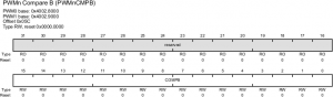
| Register | Offset |
|---|---|
| PWM0_0_CMPB | 0x05C |
| PWM0_1_CMPB | 0x09C |
| PWM0_2_CMPB | 0x0DC |
| PWM0_3_CMPB | 0x11C |
PWM generators
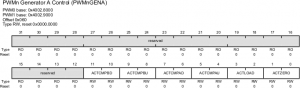
ACTCMPBD: Action when the counter matches comparator B while counting down
ACTCMPBU: Action when the counter matches comparator B while counting up
ACTCMPAD: Action when the counter matches comparator A while counting down
ACTCMPAU: Action when the counter matches comparator A while counting up
ACTLOAD: Action when the counter is reloaded
ACTZERO: Action when the counter reaches zero
For each of the above events the following actions can be choosen:
| Value | Description |
|---|---|
| 0x00 | Do nothing |
| 0x01 | Invert pwmA |
| 0x02 | Drive pwmA Low |
| 0x03 | Drive pwmA High |
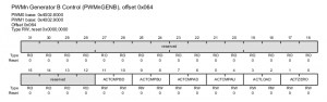
Figure 15.32 shows the offset addresses for GeneratorA and GeneratorB Control registers of PWM0 Module. We also have four GeneratorA and GeneratorB Control registers for PWM1 Module. The offset addresses are the same except the Base address for the PWM1 module is different.
| Register | Offset | Resgister | Offset |
|---|---|---|---|
| PWM0_0_GENA | 0X060 | PWM0_0_GENB | 0X064 |
| PWM0_1_GENA | 0X0A0 | PWM0_1_GENB | 0X0A4 |
| PWM0_2_GENA | 0X0E0 | PWM0_2_2GENB | 0X0E4 |
| PWM0_3_GENA | 0X120 | PWM0_3_GENB | 0X124 |
Recent Comments