
| GPIO | NVIC | SYSTICK | PLL | UART | GPTM | PWM | ADC |
| OVERVIEW | INIT&CONFIG | BLINKY | SW1&SW2 | TASKS |
Programming the GPIO in TM4C123
In this article we are going to write our first program for accessing GPIOs on the EK-TM4C123GXL LaunchPad Board.
Memory Map
The ARM Cortex-M4 has 4GB (Giga bytes) of memory space. It uses memory mapped I/O, which means that the I/O peripheral ports are mapped into the 4GB memory space.
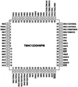
The TI EK-TM4C123GXL LaunchPad uses the TM4C123GH6PM microcontroller, which has 256K bytes (256KB) of on-chip Flash memory for code, 32KB of on-chip SRAM for data, and a large number of on-chip peripherals.
| Allocated size | Allocated address | |
|---|---|---|
| Flash | 256 KB | 0x0000.0000 To 0x0003.FFFF |
| SRAM | 32 KB | 0x2000.0000 To 0x2000.7FFF |
| I/O | All the peripherals | 0x4000.0000 to 0x400F.FFFF |
GPIO & Special Purpose I/O
While memory holds code and data for the CPU to process, the I/O ports are used by the CPU to access input and output devices. In the microcontroller we have two types of I/O :
- General Purpose I/O (GPIO)
- The GPIO ports are used for interfacing devices such as LEDs, Switches, LCD, Keypad, and so on.
- Special purpose I/O
- These I/O ports have designated function such as ADC (Analog-to-Digital), Timer, UART, PWM and so on.
TM4C123GH6PM Block Diagram
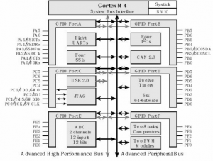
TM4C123GH6PM Micro controller
ARM chip used in TI Tiva LaunchPad is Tiva C series TM4C123GH6PM microcontroller.
The pins are designated as:
➢ PA0 – PA7
➢ PB0 – PB7
➢ PC0 – PC7
➢ PD0 – PD7
➢ PE0 – PE5
➢ PF0 – PF4
Port-E and Port-F do not have all the 8 pins implemented.
GPIO APB & AHB Bus
The ARM chips have two buses:
- Advanced Peripheral Bus (APB) and
- Advanced High-Performance Bus (AHB).
The AHB bus is much faster than APB. The AHB allows one clock cycle access to the peripherals. The APB is slower and its access time is minimum of two clock cycles.
GPIO APB Memory Map
The I/O ports addresses assigned to the Port A – Port F for APB are as follow:
- GPIO Port A : 0x4000.4000
- GPIO Port B : 0x4000.5000
- GPIO Port C : 0x4000.6000
- GPIO Port D : 0x4000.7000
- GPIO Port E : 0x4002.4000
- GPIO Port F : 0x4002.5000
GPIO AHB Memory Map
The Base addresses for the GPIOs of AHB is as follow:
- GPIO Port A : 0x4005.8000
- GPIO Port B : 0x4005.9000
- GPIO Port C : 0x4005.A000
- GPIO Port D : 0x4005.B000
- GPIO Port E : 0x4005.C000
- GPIO Port F : 0x4005.D000
4K bytes of memory space is assigned to each of the GPIO port. Each GPIO has a large number of special function registers (SFR) associated with it and the GPIO DATA register supports bit-banding. The GPIO DATA register is 8-bit wide. With bit-banding, it will need 256 words (4 bytes each, 1 KB total). There are many registers associated with each of the above I/O ports and they have designated addresses in the memory map. The above addresses are the Base addresses meaning that within that base address we have registers associated with that port.
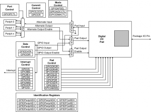
Digital I/O Pads
The TM4C123GH6PM microcontroller contains six ports and thus six of these physical GPIO blocks. Note that not all pins are implemented on every block. Some GPIO pins can function as I/O signals for the on-chip peripheral modules.
GPIO Register Map
| Name | Offset | Tivaware Name | Description |
|---|---|---|---|
| GPIODATA | 0x000 | GPIO_PORTn_DATA_R | GPIO Data |
| GPIODIR | 0x400 | GPIO_PORTn_DIR_R | GPIO Direction |
| GPIOIS | 0x404 | GPIO_PORTn_IS_R | GPIO Interrupt Sense |
| GPIOIBE | 0x408 | GPIO_PORTn_IBE_R | GPIO Interrupt Both Edges |
| GPIOIEV | 0x40C | GPIO_PORTn_IEV_R | GPIO Interrupt Event |
| GPIOIM | 0x410 | GPIO_PORTn_IM_R | GPIO Interrupt Mask |
| GPIORIS | 0x414 | GPIO_PORTn_RIS_R | GPIO Raw Interrupt Status |
| GPIOMIS | 0x418 | GPIO_PORTn_MIS_R | GPIO Masked Interrupt Status |
| GPIOICR | 0x41C | GPIO_PORTn_ICR_R | GPIO Interrupt Clear |
| GPIOAFSEL | 0x420 | GPIO_PORTn_AFSEL_R | GPIO Alternate Function Select |
| GPIODR2R | 0x500 | GPIO_PORTn_DR2R_R | GPIO 2-mA Drive Select |
| GPIODR4R | 0x504 | GPIO_PORTn_DR4R_R | GPIO 4-mA Drive Select |
| GPIODR8R | 0x508 | GPIO_PORTn_DR8R_R | GPIO 8-mA Drive Select |
| GPIOODR | 0x50C | GPIO_PORTn_ODR_R | GPIO Open Drain Select |
| GPIOPUR | 0x510 | GPIO_PORTn_PUR_R | GPIO Pull-Up Select |
| GPIOPDR | 0x514 | GPIO_PORTn_PDR_R | GPIO Pull-Down Select |
| GPIOSLR | 0x518 | GPIO_PORTn_SLR_R | GPIO Slew Rate Control Select |
| GPIODEN | 0x51C | GPIO_PORTn_DEN_R | GPIO Digital Enable |
| GPIOLOCK | 0x520 | GPIO_PORTn_LOCK_R | GPIO Lock |
| GPIOCR | 0x524 | GPIO_PORTn_CR_R | GPIO Commit |
| GPIOAMSEL | 0x528 | GPIO_PORTn_AMSEL_R | GPIO Analog Mode Select |
| GPIOPCTL | 0x52C | GPIO_PORTn_PCTL_R | GPIO Port Control |
| where n = A or B or C or D or E or F |
Accessing GPIO of this microcontroller includes much more steps as this microcontroller provides a lot of feature in a single board, hence requires lots of configuration.
For accessing and configuring the microcontroller pins, we have to load some values in the registers, associated with that particular pin.
Initialization of an I/O port
To initialize an I/O port for general use:
- Activate the clock for the port in the Run Mode Clock Gating Control Register 2 (RCGC2).
- Unlock the port (LOCK = 0x4C4F434B). This step is only needed for pins PC0-3, PD7 and PF0 on TM4C123GXL LaunchPad.
- Disable the analog function of the pin in the Analog Mode Select register (AMSEL), because we want to use the pin for digital I/O. If this pin is connected to the ADC or analog comparator, its corresponding bit in AMSEL must be set as 1. In our case, this pin is used as digital I/O, so its corresponding bit must be set as 0.
- Clear bits in the port control register (PCTL) to select regular digital function. Each GPIO pin needs four bits in its corresponding PCTL register. Not every pin can be configured to every alternative function.
- Set its direction register (DIR). A DIR bit of 0 means input, and 1 means output.
- Clear bits in the alternate Function Select register (AFSEL).
- Enable digital port in the Digital Enable register (DEN).
- Please note that we need to add a short delay between activating the clock and setting the port registers.
- PC0-PC3 is used for JTAG connections to the debugger on the LaunchPad. So we’d better do not use these pins normally.
Recent Comments