
Introduction
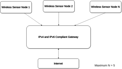
System Block Diagram
As shown in the connection diagram, the TM4123GXL board with CC110L booster pack is the sensor node in the network. It measures the parameters of interest with help of sensors and communicates the information to the gateway. The gateway is connected to internet and is able to translate between IPv4 and IPv6 packets. It receives the raw data stream sent by the sensor node and encodes it in a IPv4 TCP packet. Using the IP address of the gateway, one can receive the parameters sensed by the sensor node.
In IPv6 Gateway – part II, we have implemented the wireless connection between the sensor node and gateway. IPv6 Gateway – part I explains the TCP and web server communication details.
IPv6 Theory
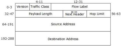
Structure of IPv6 Packet
UDP processing: UDP is a simple protocol used for demultiplexing packets between different processes. The state for each UDP session is kept in a PCB structure. The UDP PCBs are kept on a linked list which is searched for a match when a UDP datagram arrives. The UDP PCB structure contains a pointer to the next PCB in the global linked list of UDP PCBs. A UDP session is defined by the IP addresses and port numbers of the end-points and these are stored in the local ip, dest ip, local port and dest port fields.
Hardware
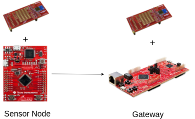
Sensor Node -> Gateway Connection
- TM4C123GXL – 2
- TM4C129EXL – 2
- Anaren CC110L Sub-1GHz Wireless Booster Pack – 2
Software Development Tools
- Eclipse Studio Environment
- OpenOCD GDB Debugger
- GtkTerm Serial Terminal
Interfacing CC110L and TM4C12XXL
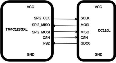
TM4C123GXL CC110L Pin Connections
SPI Interface
- The TM4C123GXL board has four SSI modules. One of the module is emulated as an SPI module and is used to connect to the CC110L chip. In our implementation for TM4C123GXL board, we have used SSI Module 2. The pin connection diagram is shown in the figure.
- The communication protocol requires CSN pin to be low during the communication. All the register accesses and read/write operations to the CC110L chip is done via SPI communication protocol.
- The CC110L chip requires the address of the register to be accessed be masked by certain bit pattern. It is as follows.
- Single Byte Read Access -> Address | 0x80
- Single Byte Write Access -> Address | 0x00
- Multiple Bytes, Burst Read Access -> Address | 0xC0
- Multiple Bytes, Burst Write Access -> Address | 0x40
- Using the above mask patterns, one writes the register address in the first cycle of the communication. In the second cycle, dummy bits are sent out of the SPI2_MOSI pin for getting data from CC110L chip.
- SPI Tx and Rx FIFO are used for sending and receiving bytes to and from chip.
CC110L Configuration
- To adhere to the ETSI European Wireless Communication standards, we have used the values specified by the CC110L RF Studio software.
- The communication is done at -0.5dBm of RF output power from CC110L chip and at ETSI 868.3MHz and FCC/IC 903MHz.
- The CC110L chip has an internal Finite State Machine (FSM) which is used by the chip to achieve packet trasmission and reception.
- The strobe commands are used to access special registers which change the states in the FSM of CC110L chip, i.e.CC1101_SRES having value 0x30u is used to put the chip in RESET state. CC1101_SIDLE with value 0x36u is used to exit RX/TX state and turns off the frequency synthesizer.
Transmitting a Packet
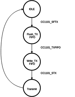
Transmit State Diagram
- The transmitting of a packet involves 4 states as shown in the figure.
- The chip is put in known state, i.e. IDLE, before beginning the transfer of packet to chip. The CC110L chip uses it’s internal TxFIFO and RxFIFO for transmitting the bytes and receiving bytes, respectively. Access to this FIFOs is through same register address 0x3F. Hence it makes the Sensor Node to Gateway communication “Half Duplex”.
- TM4C123GXL will flush the TxFIFO before sending the packet bytes to the TxFIFO. It is achieved by sending a strobe signal CC1101_SFTX. It will make sure that the bytes contained by TxFIFO are the ones Sensor Node intends to send to Gateway.
- Asserting CC1101_TXFIFO strobe will initiate the transfer of packet bytes from board to chip. These bytes will be stored in the TxFIFO in MSB first order and sent out in the same order.
- After transferring the packet bytes to TxFIFO, CC1101_STX will start the actual RF transmission of the bytes stored in TxFIFO.
- CC110L chip returns to the IDLE state once the transmission finishes without any error. It can be used as a sanity check for verifying the actual transmission.
Receiving a Packet
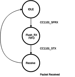
Receive Packet State Diagram
- The reception of a packet involves 3 states as shown in the figure.
- The chip is put in known state, i.e. IDLE, before beginning the reception of a packet. TM4C123GXL will flush the RxFIFO before receiving the packet bytes to the RxFIFO. It is achieved by sending a strobe signal CC1101_SFRX. It will make sure that the bytes contained by RxFIFO are the ones received from the Sensor Node.
- CC1101_SRX will make the CC110L chip open the channel and listen for the packets on it. After receiving the packet bytes to RxFIFO, the CC110L chip notifies the TM4C123GXL board by asserting the GDO0 pin low. The GPIO falling edge Interrupt Service Routine will read the bytes from the RxFIFO and store it in the memory.
- CC110L chip returns to the IDLE state once the reception finishes without any error.
Future Work
- Integration of multiple Sensor Nodes to a Gateway; Mesh Network Implementation
- LwIP implementation at the network layer in communication
- SenseHub Booster Pack integration for different sensors
- Link Performance and Communication Parameters Calculation
Team
- Ankit Zalawadiya
- Neha Rangari
Recent Comments