
Hardware Interface Programming
| Keypad | 7seg display | LCD | SPI | I2C |
| INTRODUCTION | SPI IN TIVA | SPI DAC | SPI SAMPLES | SPI TASKS |
SPI programming in TI ARM Tiva
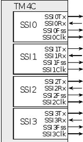
The TM4C123GH6PM microcontroller system includes four Synchronous Serial Interface modules (SSI0, SSI1, SSI2 and SSI3). Each SSI module provides a master or a slave interface for synchronous serial communication (SSI) with peripheral devices that have either Freescale SPI, MICROWIRE, or Texas Instruments synchronous serial interfaces (SSI). The SSI modules are located at the following base addresses:
| SSI Module | Base Address |
|---|---|
| SSI0 | 0x40008000 |
| SSI1 | 0x40009000 |
| SSI2 | 0x4000A000 |
| SSI3 | 0x4000B000 |
The SSI protocol includes four I/O lines:
- The slave select SSI0Fss is an optional negative logic control signal from master to slave signal signifying the channel is active.
- The second line, SSI0Clk, is a 50% duty cycle clock generated by the master.
- The SSI0Tx (master out slave in, MOSI) is a data line driven by the master and received by the slave.
- The SSI0Rx (master in slave out, MISO) is a data line driven by the slave and received by the master.
In order to work properly, the transmitting device uses one edge of the clock to change its output, and the receiving device uses the other edge to accept the data.
On the TM4C the shift register can be configured from 4 to 16 bits. The shift register in the master and the shift register in the slave are linked to form a distributed register. The following figure illustrates communication between master and slave.
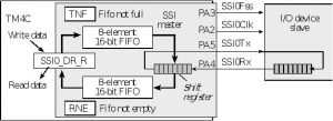
Typically, the micro controller and the I/O device slave are so physically close we do not use interface logic. The SSI on the TM4C employs two hardware FIFOs. Both FIFOs are 8 elements deep and 4 to 16 bits wide, depending on the selected data width. When performing I/O the software puts into the transmit FIFO by writing to the SSI0_DR_R register and gets from the receive FIFO by reading from the SSI0_DR_R register. If there is data in the transmit FIFO, the SSI module will transmit it. With SSI it transmits and receives bits at the same time. When a data transfer operation is performed, this distributed 8- to 32-bit register is serially shifted 4 to 16 bit positions by the SCK clock from the master so the data is effectively exchanged between the master and the slave. Data in the master shift register are transmitted to the slave. Data in the slave shift register are transmitted to the master. Typically, the micro controller is master and the I/O module is the slave, but one can operate the micro controller in slave mode.
The SPI transmits data at the same time as it receives input. In the Freescale modes, the SPI changes its output on the opposite edge of the clock as it uses to shift data in. There are three mode control bits (MS, SPO, SPH) that affect the transmission protocol. If the device is a master (MS=0) it generates the SCLK, and data is output on the SSI0Tx pin, and input on the SSI0Rx pin. The SPO control bit specifies the polarity of the SCLK. In particular, the SPO bit specifies the logic level of the clock when data is not being transferred. The SPH bit affects the timing of the first bit transferred and received. If SPH is 0, then the device will shift data in on the first (and 3rd, 5th, 7th, … etc.) clock edge. If SPH is 1, then the device will shift data in on the second (and 4th, 6th, 8th, … etc.) clock edge. The data is transmitted MSB first.
![]()
Enabling Clock to SSI
To enable and use any of the peripheral modules in the Tiva chip, we must enable the clock to it. We use RCGCSSI register to enable the clock to SSI modules. Notice again RCGCSSI is part of the SYSCTL registers. Writing a one to each of the R3 to R0, enables the corresponding SSI module. We need RCGCSSI = 0x0F to enable the clock to all four SSI modules.
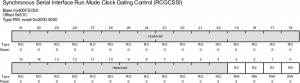
| Bit/Filed | Name | Description |
|---|---|---|
| 0 | R0 | SSI Module 0 Run Mode Clock Gating Control 0: SSI module 0 is disabled. 1: Enable and provide a clock to SSI module 0 in Run mode. |
| 1 | R1 | SSI Module 1 Run Mode Clock Gating Control 0: SSI module 1 is disabled. 1: Enable and provide a clock to SSI module 1 in Run mode. |
| 2 | R2 | SSI Module 2 Run Mode Clock Gating Control 0: SSI module 2 is disabled. 1: Enable and provide a clock to SSI module 2 in Run mode. |
| 3 | R3 | SSI Module 3 Run Mode Clock Gating Control 0: SSI module 3 is disabled. 1: Enable and provide a clock to SSI module 3 in Run mode. |
Configuring the SSI Module
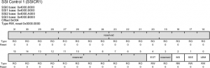
The SSICR0 (SSI Control register 0) sets SSI configuration. The following figure shows the bits of SSICR0 and the table describes the function of each bit. Although the conventional SPI uses only 8-bit data, the SSI modules allow transfer of data between 4 bits to 16 bits.
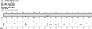
| Bits/Fields | Name | Function | Description |
|---|---|---|---|
| 0-3 | DSS | SSI Data Size Select | 0x0000: Reserved 0x0001: Reserved 0x0010: Reserved 0x0011: 4-bit data, 0x0100: 5-bit data, 0x0101: 6-bit data, 0x0110: 7-bit data, 0x0111: 8-bit data 0x1000: 9-bit data, 0x1001: 10-bit data, 0x1010: 11-bit data, 0x1011: 12-bit data, 0x1100: 13-bit data 0x1101: 14-bit data, 0x1110: 15-bit data, 0x1111: 16-bit data |
| 4-5 | FRF | SSI Frame Format Select | 0x00: SPI, 0x01: TI, 0x10: MICROWIRE frame format and 0x11: Reserved |
| 6 | SPO | SSI Serial Clock Polarity (Only works for Freescale SPI Frame) |
0: The inactive level for the SSInClk pin is Low. 1: The inactive level for the SSInClk pin is High. Note: If this bit is set, the software must also configure the GPIO port pin corresponding to the SSInClk signal as a pull-up in the GPIO Pull-Up Select ( GPIOPUR) register. |
| 7 | SPH | SSI Serial Clock Phase (Only work for Freescale SPI Frame) |
0: Data is captured on the First clock edge transition. 1: Data is captured on the Second clock edge transition. |
| 8-15 | SCR | SSI Serial Clock Rate | This bit field is used to generate the transmit and receive bit rate of the SSI (0–255) BR=SysClk/(CPSDVSR * (1 + SCR)) |
Setting Bit Rate
SSI module clock source can be either of System Clock or PIOSC (Precision Internal Oscilator). The selected frequency is fed to prescaler before it is used by the Bit Rate circuitry, as shown in the following figure.
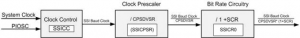
The CPSDVSR (CPS Divisor) value comes from the prescaler divisor register shown in the following figure.
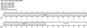
The lower 8 bits of SSICPSR (SSI Clock Prescale) register are used to divide the CPU clock before it is fed to the Bit Rate circuitry. Only even values can be used for the prescaler since the D0 must be 0. For the prescaler register, the lowest value is 2 and the highest is 254.
The SSICR0 (SSI Control register 0) allows the Bit Rate selection among other things. The output of clock prescaler circuitry is divided by 1 + SCR and then used as the SSI baud rate clock. The value of SCR can be from 0 to 255.
We can use the following formula to calculate the Bit Rate (BR):
BR=SysClk/(CPSDVSR × (1 + SCR))
Example 1: Assume the prescaler register has SSICPSR=0x20 and system clock frequency is 16MHz. Find the values for the SCR part of the SSOCR0 register for the bit rate of (a) 100K, (b) 250K, and (c) 500K.
Solution: Since the prescaler is 0x20 (32 in decimal), we have 16MHz / 32 = 500KHz. Now:
(a) 16MHz / (32 x (1 + 4)) = 100KHz.
(b) 16MHz / (32 x (1 + 1)) = 250KHz.
(c) 16MHz / (32 x (1 + 0)) = 500KHz.
Example 2: In a given program, we have Bit Rate=50KHz and SCR=03 in SSICR0 register. Find the prescaler register value if system clock frequency is 16MHz.
Solution:
BR = SysClk / (CPSDVSR × (1 + SCR))
50KHz = 16MHz / (X × (1 + 3). Now, the prescaler value is 80 in decimal or 0x50 in Hex. Therefore the SSICPSR = 0x50.
Other SPI configurations
The D3-D0 bits of SSICR0 are used to select the data size. In most cases, we use 8-bit data size. The bits 5-4 are used to select various protocols. Upon Reset, the default protocol is Freescale SPI.
Example 3: In example 1, find the values for the control register SSICR0 register if we want the Freescale SPI with 8-bit data size and SPH=1, SPO=1.
Solution:
(a) SSICR0=00000100 00110111 in binary or = 0x437. Notice, we have set SPH and SPO bits to 1.
(b) 0x137, and
(c) 0x037.
Master or Slave?
The SSI Module inside the Tiva chip can be Master or Slave. We use MS bit in SSI control register 1 (SSICR1) to designate the Tiva chip as master or slave. Another important bit in the SSICR1 register is enable/ disable bit (SSE). We must disable SSIx module during the initialization process and enable it afterward.
| Bit | Name | Function | Description |
|---|---|---|---|
| 0 | LBM | SSI Loopback Mode | 0: Normal serial port operation enabled. 1: Output of the transmit serial shift register is connected internally to the input of the receive serial shift register. |
| 1 | SSE | SSI Synchronous Serial Port Enable | 0: SSI operation is disabled. 1: SSI operation is enabled. This bit must be cleared before any control registers are reprogrammed. |
| 2 | MS | SSI Master/Slave Select | Select Master or Slave mode 0: The SSI is configured as a Master. 1: The SSI is configured as a Slave. Note: Can be modified only when the SSI is disabled (SSE = 0) |
| 3 | Reserved | – | – |
| 4 | EOT | End Of Transmission | This bit is only valid for Master mode devices and operations (MS = 0x0) 0: The TXRIS interrupt indicates that the transmit FIFO is half-full or less. 1: The End of Transmit interrupt mode for the TXRIS interrupt is enabled. |
| 31:5 | Reserved | – | – |
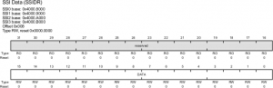
Data Register
The data is placed in SSIDR (SSI Data register) for transmission. The SSIDR is also used for the received data buffer. In 8-bit data size selection, we must place the data into the lower 8-bits of the register and the rest of the register are unused. In the receive mode, data is right-justified meaning the lower 8-bit holds the received data.
Status Flag Register
We use the SSI Status flag register (SSISR) to monitor to see whether a byte has been received or if the transmission buffer is empty and ready for the next byte to be transmitted.
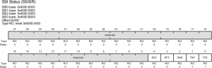
| Bits | Name | Function | Description |
|---|---|---|---|
| 0 | TFE | SSI Transmit FIFO Empty | The bit is 1 when the transmit FIFO is empty |
| 1 | TNF | SSI Transmit FIFO Not Full | The bit is 1 when the SSI transmit FIFO not full |
| 2 | RNE | SSI Receive FIFO Not Empty | The bit is 1 when the receive FIFO is not empty |
| 3 | RFF | SSI Receive FIFO Full | The bit is 1 when the receive FIFO is full |
| 4 | BSY | SSI Busy Bit | The bit is 1 when the SSI is currently transmitting or receiving |
Interrupt using NVIC
We can use an interrupt handler to do the job of transmit and receive. By enabling the interrupt bits in SSIIM (SSI Interrupt Mask) register, we direct the interrupt to the NVIC interrupt controller and write an interrupt handler. Upon Reset, the interrupts are masked and raising of the flag will not direct it to NVIC.
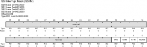
| Bits | Name | Function | Description |
|---|---|---|---|
| 0 | RORIM | SSI Receive Overrun Interrupt Mask | The receive FIFO overrun interrupt is masked when RORIM is zero and not masked when it is one |
| 1 | RTIM | SSI Receive Time-Out Interrupt Mask | The receive FIFO time-out interrupt is masked when RTIM is zero and not masked when it is one |
| 2 | RXIM | SSI Receive FIFO Interrupt Mask | The receive FIFO interrupt is masked when RXIM is zero and not masked when it is one |
| 3 | TXIM | SSI Transmit FIFO Interrupt Mask | The transmit FIFO interrupt is masked when TXIM is zero and not masked when it is one |
Recent Comments