
Objective
The objective of this project is to implement an embedded system that can be used for edge computing. It should be capable of the following tasks:
- Process inputs in real-time
- Perform fast computation
- Provide condensed and vital information to the higher layer
This project uses Handwritten digit recognition as an application to demonstrate the use of microcontrollers in the edge domain.
NOTE: Due to unavailability of the board, this project was implemented only through Simulation in Keil µVision 5 Tool.
Motivation

In the traditional sensor network architecture, the sensors are only used and data acquisition modules and all computation happens at the cloud. Edge computing has the following advantages over the traditional model:
- Bandwidth reduction – transmitting only essential information to higher levels.
- Efficiency and Speed – processing at sensor nodes eliminates propagation delays, errors and requirement of signal boosters. Provides real-time assistance.
- Security and Privacy – information is contained within one node and full information is not relayed.
There are a few challenges in the path to harness the above advantages:
- Limited resources – need to optimise computation, reduce memory footprint due to less-powerful processors and small memories.
- Algorithm restructuring – need to handle asynchronous requests that are priority-based, without skipping input capture.
This project explores several techniques to reduce the memory and computational footprint of neural networks in order to fit into the microcontroller.
System Overview
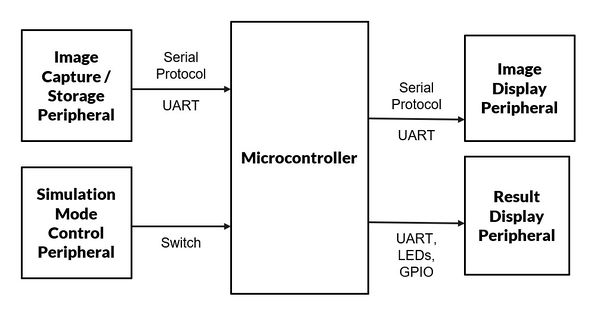
Inputs:
- UART: The microcontroller takes input images through UART.
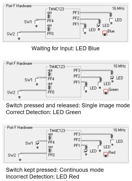
- Switch: Control is provided to the user through the on-board switch regarding the mode of transfer, which can be
-
- Single image transfer mode – Switch press and release
- Continuous transfer mode – Keep switch pressed
Outputs:
- UART: The input image, expected digit and predicted digit are displayed on the Serial terminal through UART.
- LEDs: The operation mode and result of the batch testing is shown in the LEDs, as
-
- Blue – if waiting for image
- Green – if all images detected correctly
- Red – if one or more images detected incorrectly
HW and SW Tools
- Target Board:
- TM4C123GH6PM (Texas Instruments TIVA C Series)
- ARM Cortex-M4
- 256 KB Flash, 32 KB RAM
- Due to unavailability of the board, only simulation was done.
- Simulation Platform:
- Keil µVision5 Microcontroller Development Kit (MDK Version 5) by ARM
- Only Network Inference is implemented in the simulation.
- Image Dataset:
- MNIST
- Neural Network Training:
- Python
Neural Network Implementation
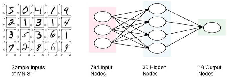
(Network Image Source: https://blog.goodaudience.com/artificial-neural-networks-explained-436fcf36e75)
MNIST Dataset is used for training and testing the network. Input images are 28×28 grayscale (0-255) format, having handwritten single digits 0 – 9. MNIST contains 60000 training samples and 10000 test samples.
The images are linearized and provided to 784 input nodes. 30 nodes are used in the hidden layer. The output layer has 10 nodes, one for each digit. A max-classifier follows the output layer to choose the digit with the maximum output as the predicted result. Rectified Linear Unit (ReLU) activation is used for all nodes, as it is easily implementable on hardware and avoids the vanishing gradient problem.
Data Optimizations
The following data optimizations are incorporated in the implementation in order to reduce the memory footprint, latency and the computation time.
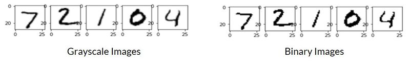
Input Binarization:
MNIST images are of 8-bit (grayscale) format with size 28 x 28. Since input images are black and white, the 8-bit pixel value (from 0 to 255) is converted to single bit value by midway thresholding (using 128 as threshold). The advantages of input binarization are as follows:
- Reduced memory usage: Input memory reduced by 87.5%.
- Multiplier-less 1st layer: Since inputs are binary, the product of input and first layer weights is either 0 or the weight itself which reduces computation.
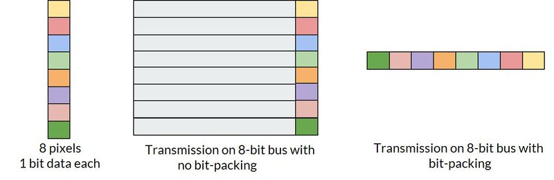
Bit-packing:
Since UART does byte transfer, 8 bits corresponding to 8 pixels are packed into a single transfer. The advantage of this technique is that it reduces the number of UART transfers from 784 to 98 which causes further reduction in input latency by 87.5%.
Fixed point implementation:
Although floating point format gives a good dynamic range, calculations involving floating point numbers are complex to implement on hardware. The algorithm is thus converted to its fixed-point equivalent as training ensures good accuracy of results even with reduced-precision computing.
q7 format (7 fractional bits, 1 sign bit) is used with integer bits varying from 0 (int8 data type) to 7 (int16 datatype).
Training Results
Memory Requirements:
- Weights: Input to hidden layer weights require 784 X 30 bytes for storage and 30 X 10 bytes are utilized for storing hidden to output layer weights which adds up to a total of 26.26KB for storing the weights of the neural network.
- Arrays for storing input, hidden and output layers: The input values are 98 in number in int8 format while the hidden and output layer have 30 and 10 values respectively in int16 format which gives a total of 178 bytes.
Transfer requirements:
Transfer is done in HEX format through UART. Each image is sent in 98 transfers bytewise.
UART Simulation
Debugger Initialization File
Debugger Initialization File with extension .ini is used to model the external hardware. Inputs assigned through the microcontroller pins are available in Keil tool as virtual simulation registers (VTREG). DIR VTREG command is used to see the list of virtual registers in command window in Debug mode on Keil. The list of few of the available virtual registers are as shown in figure below.
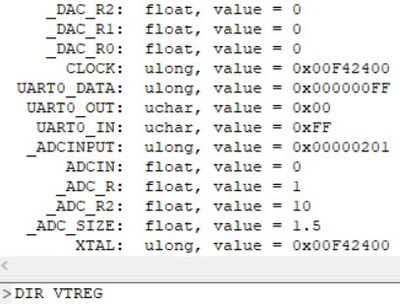
UART0_IN and PORTF are the virtual registers used to give inputs through UART0 and GPIO Port F respectively. Incase of UART input, the datatype used is uchar (unsigned char), which accepts 8 bit hexadecimal number.This is a way to provide binary inputs and values that exceed 7 bits and thus cannot be given in ASCII representation.
Simulation Script
A test script is generated to provide input images through UART, as shown in the below figure.
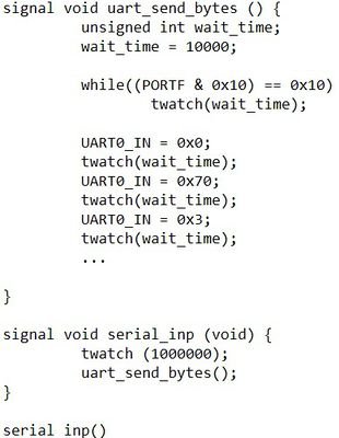
Signal functions are used to simulate and test the port communications, serial and analog I/Os and other external events which are repetitive in nature. These functions repeat the operations in the background while the target program is being run by Keil µVision tool. Signal functions start with keyword ‘signal’ and have void return type.
The image input is sent bytewise (8 pixels at once) in hexadecimal format. ‘twatch’ function reads the processor clock and delays by the specified number of clock cycles. Appropriate delay is to be given before sending input through UART to ensure that UART, GPIOs are initialized and the neural network is reset. A while loop is added to wait for the user to toggle switch S1 (GPIO Port F pin 4) before sending the next image.
Algorithm
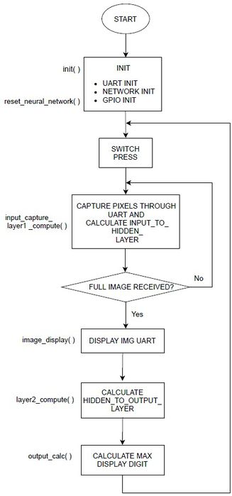
The algorithm implemented is as shown in flowchart above. The functions used in the implemented code are as mentioned in the flowchart.
- init() function initializes the registers associated with UART and GPIO PortF and reset_neural_networks() resets the neural network outputs to 0 before taking in input.
- On pressing the switch, input_capture_layer1_compute function captures the pixels through UART and computes the inputs to the hidden layer. This process repeats until full image is received.
- Once the entire image is received, the image is displayed through UART by image_display() function.
- layer2_compute() function uses ReLU activation and multiplier-less quantization to compute the inputs to the output layer.
- The maximum of the output digit is computed by output_calc() function followed by the display of expected and predicted digit.
Simulation Results
Accuracy:
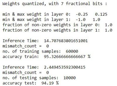
Classification Accuracy on test set is obtained as 94.19%.
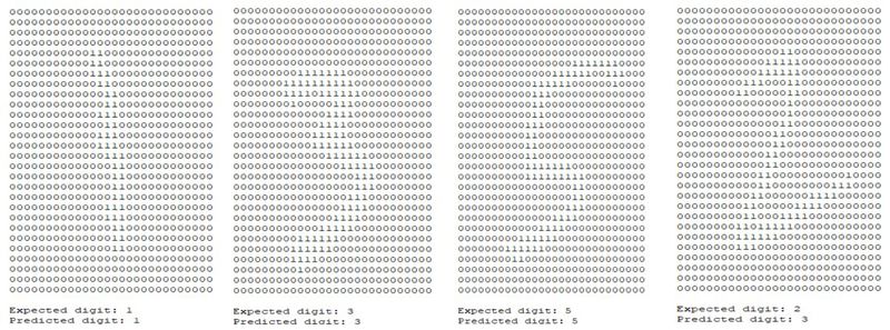
UART Output:
The following images show the printed digit, with the expected and predicted values, as displayed on the Serial Terminal in Keil.
LED and Switch:
The LED and Switch user interface, provided by the Launchpad library on Keil, is shown below, for different operating modes and results.
Learnings and Future Work
The project provided us with the following learning outcomes:
- Design and optimization of a neural network for a resource-constrained embedded system.
- Usage of Keil µVision5 Tool – Building, Debugging, Simulation.
- Debugger initialization file development methodology.
Future work on the Hardware front:
- Integrate a camera with the board for real time image processing, through SPI /I2C protocol.
- Inputs can be read by external storage devices through SPI / I2C protocol.
- Output image can be displayed on an LCD panel through SPI / I2C protocol.
- Interrupt-driven system can be designed.
Future work on the Algorithm front:
- The training can be expanded to alphanumeric characters.
- Input trackpad can be used to write the digit, to make it a smart slate, that converts handwritten notes into digital documents.
- Training can be done for Indic languages.
References
Neural Network:
- MNIST Dataset: http://yann.lecun.com/exdb/mnist/
- Python Machine Learning Tutorial: https://www.python-course.eu/neural_network_mnist.php
Introduction to Keil:
- The Designer’s Guide to the Cortex-M Processor Family (2nd Edition) – Trevor Martin
- UART Project:
Simulation file creation:
Recent Comments