
Introduction:
Dot LED matrices are a cheap and easy to use hardware. They are commonly used as
display signs and are often appreciated for their long-range visibility and cost-effective solution
for advertising purposes. These Dot LED matrices are configured using MAX 7219 driver. In
this project 4 Dot LED matrices are cascaded to display a scrolling text characters. The user
has control over quite a few features of the text which will be discussed in the subsequent
sections. The idea is to learn about MAX 7219 driver and use SSI0 hardware built in the
processor and the driver to trigger serial communication between the two for data transfers
which will be displayed as characters on the Dot LED matrix display.
1. Circuit and wiring diagram:
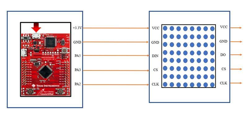
Figure 1:Circuit and wiring diagram
Implementation Details
Initializing GPIO Port-F:
GPIO PortF is configured to take inputs from hardware switches that are internally
mapped. The SW1 and SW2 switches are connected to PF4 and PF0, respectively. These
switches will be used in the program to trigger interrupts. The GPIO PortF ISR will take
of the scroll speed and display intensity. The initialization of PortF for this purpose is
mentioned below:
1. Enabling System clock to PortF through SYSCTL_RCGC2_R register.
2. Unlocking PortF through GPIO_PORTF_LOCK_R register.
3. Set the GPIO Commit register to allow changes in PortF through
GPIO_PORTF_CR_R register.
4. Disable the analog mode for PortF in GPIO_PORTF_AMSEL_R register.
5. Set the directions of all the 5 PortF pins using the GPIO_PORTF_DIR_R register,
PF4 and PF0 are set as input pins (inputs are set to 0 in the control word).
6. Once the directions are set, pull up resistors are enabled for PF4 and PF0 using
GPIO_PORTF_PUR_R register.
7. Disable the alternate functionality for all pins in PortF using GPIO_PORTF_AFSEL_R
register.
8. Enable digital mode in PF4, PF0 using the GPIO_PORTF_DEN_R register.
9. PortF Interrupt is enabled and configured to sense it at the falling edge.
Port-F Interrupt Handler:
1. Once SW1 and SW2 are configured to be interrupts, the handler is programmed to
detect SW1 and SW2. SW2 controls the intensity of the display. SW1 controls the
word to be displayed.
2. When a particular switch is detected corresponding interrupt flag is cleared and the
corresponding check flag is set.
3. The check flag status is checked in the main program in the infinite while loop.
4. When SW1 is pressed, PortF_SW1_INTR flag is set and the word being displayed
is changed (in other words, global variable index is changed).
5. When SW2 is pressed, PortF_SW2_INTR flag is set the Dot matrix is re-initialized
with the modified intensity.
Initializing GPIO Port-C and E:
GPIO Port-C and E are configured to take inputs from KeyPad switches that are
internally mapped. To reduce the microcontroller, I/O pin usage, keyboards are organized
in a matrix of rows and columns. The CPU accesses both rows and columns through ports;
therefore, with two 8-bit ports, an 8×8 matrix of 64 keys can be connected to amicroprocessor.
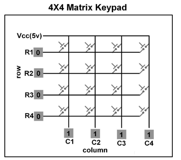
Figure 2 : 4×4 keypad
Keys on a keyboard are organized in a matrix of rows and columns. The
microcontroller accesses both rows and columns through GPIO ports. When a key is
pressed, a row and a column make contact to detect the key.
In EduARM board, the rows are connected to an output port (PE0 – PE4) and the
columns are connected to an input port (PC4 – PC7). All the input pins should have pull-
up resistor connected (select an internal pull-up resistor). If no key has been pressed,
reading the input port will yield 1s for all columns. If all the rows are driven low and a
key is pressed, the column of that key will read back a 0 since the key pressed shorted
that column to the row that is driven low. It is the function of the microprocessor to scan
the keyboard continuously to detect and identify the key pressed.
These switches will be used in the program to trigger interrupts. The GPIO PortC
ISR can be used to set the status of the display. The following functionalities can be
achieved using the Keypad.
1. SW (1,1) →Switch between different strings
2. SW (1,2)→Increase LED Brightness
3. SW (1,3)→Decrease LED Brightness
4. SW (2,1)→Left Scrolling
5. SW (2,2)→Right Scrolling
6. SW (2,3)→Scroll Off
7. SW (3,1)→Increase Scrolling Speed
8. SW (3,2)→Decrease Scrolling Speed
9. SW (3,2)→Switch ON Blinking the Text
10. SW (3,2)→Switch OFF Blinking the Text
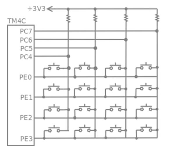
Figure 3:EduARM4 Trainer Board – 4×4 keypad
The initialization of Port C for this purpose is mentioned below:
1. Enabling System clock to Port C and E through SYSCTL_RCGC2_R register.
2. Set the directions of Port – C (PC7 – PC4) pins and Port – E (PE3 – PE0) pins using
the GPIO_PORTC_DIR_R and GPIO_PORTE_DIR_R registers respectively.
PC7-PC4 are set as input pins and PE3-PE0 are set as output pins.
3. Once the directions are set, pull up resistors are enabled for PC7-PC4 using
GPIO_PORTC_PUR_R register. PE3-PE0 pins are configured as open drain output
(which means they are driven low actively but not driven high) using
GPIO_PORTE_ODR_R register.
4. PE3-PE0 pins are used for rows and configured as output digital pins using
GPIO_PORTE_DEN_R register. PC7-PC4 pins are configured as input digital pins
with the internal pull-up resistors enabled using GPIO_PORTC_DEN_R register.
5. Port C Interrupt is enabled and configured to sense it at the falling edge.
4.
Port C Interrupt Handler:
1. PC7-PC4 are configured to be interrupts, the handler is programmed to detect them.
2. Whenever a key is pressed, the GPIOPortC_Handler function is called and if the
configured key press is detected, then Keypad_INTR_flag will be set.
3. The character variable input stores the Pressed Key status.
4. Inside the while loop of the main program Keypad_INTR_flag is checked for true
condition, when it becomes true, the set_display_status function is called. It checks if
the input from keypad is valid or not and corresponding task is performed.
5.
Initializing UART0:
UART0 is configured to control the Dot Matrix through the UART console. UART0
supports a set of commands namely:
1. change→Switch between different strings
2. bright→Increase LED Brightness
3. dim→Decrease LED Brightness
4. scroll left→Left Scrolling
5. scroll right→Right Scrolling
6. scroll off→Scroll Off
7. inc speed→Increase Scrolling Speed
8. dec speed→Decrease Scrolling Speed
9. blink on→Switch ON Blinking the Text
10. blink off→Switch OFF Blinking the Text
11. data→To give input data from UART
The entered key word is matched against the above-mentioned commands and
executes the corresponding task in a function named set_display_status. UART0 is
configured to trigger an interrupt every time a key is pressed on the keyboard. This is
achieved by setting the below mentioned registers:
1. Enabling clock for UART0 through SYSCTL_RCGCUART_R register.
2. As UART0 Rx and Tx are enabled through Alternate functionality of GPIO Port A,
clock should be enabled for GPIO Port A through SYSCTL_RCGCGPIO_R register.
3. Alternate functionalities of PA0, PA1 are enabled to allow UART0 Rx and Tx, through
GPIO_PORTA_AFSEL_R register.
4. UART0 Tx and Rx are configured to a Baud Rate of 11520, without parity, 1 start bit
and 1 stop bit by setting appropriate registers.
5. UART0 interrupt is enabled in the NVIC and set to a priority of 5.
6. TXIM bit is set in the UART0_IM_R register to detect interrupt on the UART0 Tx
channel.
6.
UART0 Interrupt Handler:
1. When a key is pressed on the keyboard, an interrupt is triggered.
2. In the interrupt handler, the pressed key is stored in a temporary variable and
transmitted back to the console where the character entered is printed.
3. If the key pressed is an alphabet or a number or a special character, then it will be stored
in a globally defined buffer.
4. When Enter key is pressed, UART_INTR_flag is set.
5. Inside the while loop of the main program UART_INTR_flag is checked for true
condition, when UART_INTR_flag becomes true, the set_display_status function is
called. It checks if the command (buffer) entered is valid or not and corresponding task
is performed.
7.
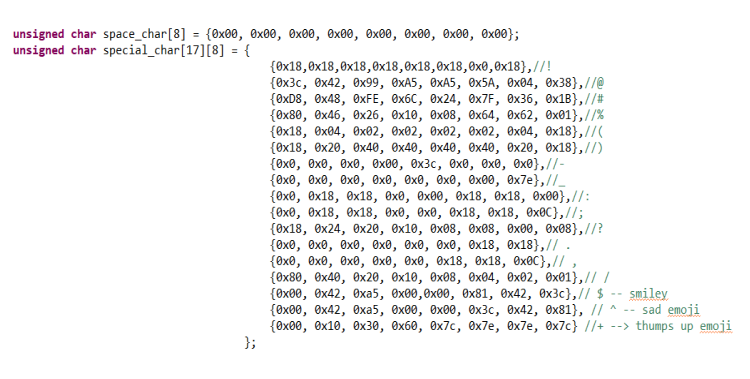
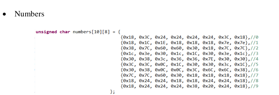
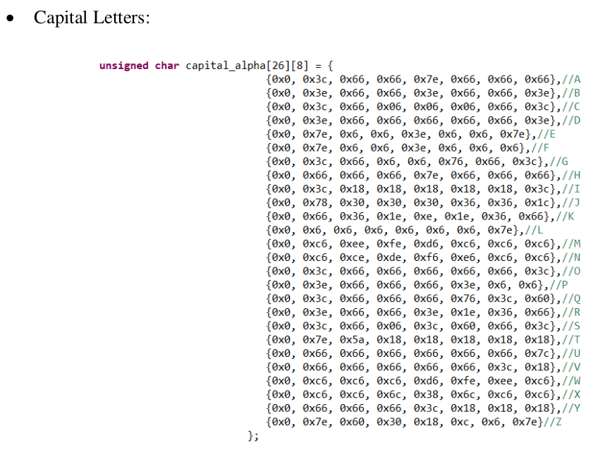
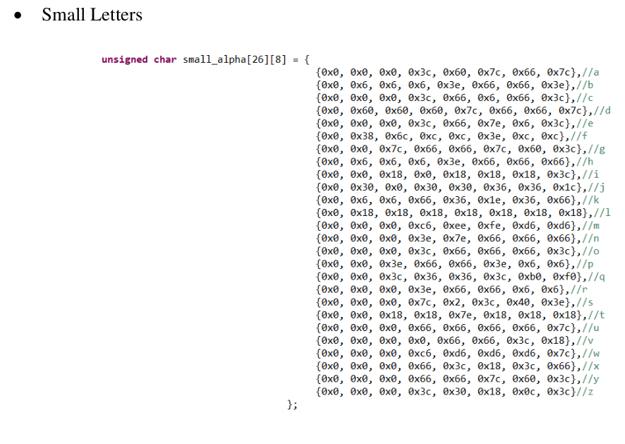
Characters Supported:
•
Special Characters
8.
LED Dot Matrix Display
In a LED dot matrix display the LEDs are located at the column and row
intersections of the matrix. LEDs in the same row are connected as are LEDs in the
same column. Figure 4 shows common cathode configurations for LED matrix display
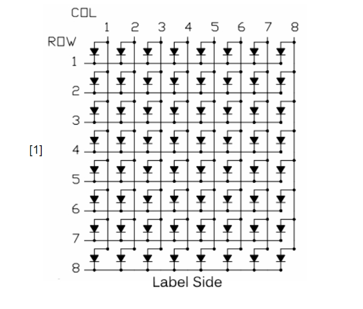
Figure 4: common cathode configurations for LED matrix display
9.
MAX7219 Driver
MAX7221 segment drivers are slew-rate limited to reduce electromagnetic
interference (EMI), and its serial interface is fully SPI compatible.
•
Initial Power-Up
On initial power-up, all control registers are reset, the display is blanked, and the
MAX7219 enter shutdown mode. Program the display driver prior to display use.
Otherwise, it will initially be set to scan one digit, it will not decode data in the data
registers, and the intensity register will be set to its minimum value.
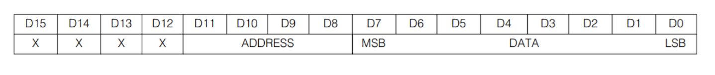
Table 1: Serial-Data Format (16 bits)
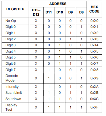
Table 2: Register Address M
Table 2 lists the 14 addressable digit and control registers. The control registers
consist of decode mode, display intensity, scan limit (number of scanned digits), shutdown,
and display test (all LEDs on).
•
Initialising MAX7219 driver:
o Setting up scan limit Register
▪ To select all rows of led dot matrix we set scan register to 0b07.
o Setting up Shutdown Register
▪ Table: Shutdown Register Format (Address (Hex) = 0xXC)
▪ Here MAX7219 is operated in Normal Operation mode.
o Setting up Intensity Register
▪ Table: Intensity Register Format (Address (Hex) = 0xXA)
▪ Intensity can be controlled in 16 discrete steps from 0x0 to 0xf.
10.
Synchronous Serial Interface (SSI)
In TM4C123GH6PM MCU system, the SPI is used to work as a synchronous
serial interface. Two devices communicating with synchronous serial interfaces (SSI)
operate from the same clock (synchronized). With a SSI protocol, the clock signal is
included in the interface cable between devices. Typically, the master device creates
the clock, and the slave device(s) uses the clock to latch the data in and send data out.
SPI devices use only 2 pins for data transfer, called SDI (Din) and SDO (Dout).
This reduction of data pins reduces the package size and power consumption drastically,
making them ideal for many applications in which space is a major concern. The SPI
bus has the SCLK (serial clock) pin to synchronize the data transfer between two chips.
The last pin of the SPI bus is CE (chip enable), which is used to initiate and terminate
the data transfer. These four pins, SDI, SDO, SCLK, and CE, make the SPI a 4-wire
interface. In many chips, the SDI, SDO, SCLK, and CE signals are alternatively named
as MOSI (Master Out Slave In), MISO (Master In Slave Out), SCK, and SS.
Initialising SSI0:
Step 1: To activate SSI
•
SYSCTL_RCGCSSI_R = 0x01;
RCGCSSI: Synchronous Serial Interface Run Mode Clock Gating Control. The
RCGCSSI register provides software the capability to enable and disable the SSI modules
in Run mode. When enabled, a module is provided a clock and accesses to module registers
are allowed. When disabled, the clock is disabled to save power and accesses to module
registers generate a bus fault.
Step 2: Activating port A
•
RCGCGPIO: General-Purpose Input/Output Run Mode Clock Gating Control
The RCGCGPIO register provides software the capability to enable and disable
GPIO modules in Run mode. When enabled, a module is provided a clock and accesses to
module registers are allowed. When disabled, the clock is disabled to save power and
accesses to module registers generate a bus fault.
Step 3: Enabling alternate functionality on PA2,3,5
•
GPIO_PORTA_AFSEL_R |= 0x2C;
Here PA2 is connected to Clk of MAX7219 Driver and PA3 to CS and PA5 to data
in of driver. Data out of first led matrix is given as data into next led dot matrix display.
Step 4: Enabling digital Input/Output on PA2,3,5
•
GPIO_PORTA_DEN_R |= 0x2C;
Step 5: Configure PA2,3,5 as SSI
•
GPIO_PORTA_PCTL_R = (GPIO_PORTA_PCTL_R & 0xFF0F00FF) + 0x00202200;
GPIO Port Control (GPIOPCTL) register which selects one of several peripheral
functions for each GPIO.
Step 6: Disabling analog functionality on Port A
•
GPIO_PORTA_AMSEL_R = 0;
Step 7: Disabling SSI
•
SSI0_CR1_R &= ~SSI_CR1_SSE;
This bit must be cleared before any control registers are reprogrammed.
Step 8: Configuring SSI as Master
•
SSI0_CR1_R &= ~SSI_CR1_MS;
The SSI is configured as a master.
Step 9: Setting clock polarity and phase to 0
•
SSI0_CR0_R &= ~(SSI_CR0_SCR_M | SSI_CR0_SPH | SSI_CR0_SPO);
Step 10: Selecting free scale format
•
SSI0_CR0_R = (SSI0_CR0_R & ~SSI_CR0_FRF_M) +SSI_CR0_FRF_MOTO;
Step 11: Selecting data width
•
SSI0_CR0_R = (SSI0_CR0_R & ~SSI_CR0_DSS_M) + SSI_CR0_DSS_16;
Step 12: Clock divider for 1.6 MHz SSI Clock (assumes 16 MHz PLL)
•
SSI0_CPSR_R = (SSI0_CPSR_R & ~SSI_CPSR_CPSDVSR_M) + 10;
Step 13: Enabling SSI
•
SSI0_CR1_R |= SSI_CR1_SSE;
Programmed SSI0 to Free scale format, 16bit transfer, 0 polarity and 0 phase, clock
speed 1.6MHz.
SSI0_WRITE:
Step 1: Disabling Interrupts
•
Disable_interrupts ();
Step 2: Choosing SSI0
•
GPIO_PORTA_DATA_R &= ~0x08;
Step 3: Waiting until FIFO is full and transmitting data through SSI
•
•
while ((SSI0_SR_R & 2) == 0); /* wait until FIFO not full */
SSI0_DR_R = data; /* transmit high byte */
Step 4: Waiting until transmission is done by monitoring status register
•
•
while (SSI0_SR_R & 0x10); /* wait until transmit complete */
GPIO_PORTA_DATA_R |= 0x08; /* keep SS idle high */
Step 5: Enabling Interrupts
•
Enable_interrupts ();
Functionality
GPIO Ports (A, C, E, F), UART0, SSI0 and the Dot matrix drivers are initialized and
the characters to be displayed are globally defined.
Once the strings to be displayed are defined, the characters are identified, and the
related data are stored in separate buffers. All of this is done in encode_char function. These
buffers contain the row data of all characters. In the main program, scroll_data and
write_led_data functions are called in a while loop.
Inside the scroll_data function, scroll flag is checked for various conditions. If scroll
flag is ‘1’, the row data is shifted left and if it is ‘2’ the row data is shifted right and if it is ‘0’
zero, the same row data is copied. The updated data is stored in globally defined encoded_data
matrix. The encoded_data is sent through SSI0_write function.
To control the speed of scroll, a global variable is defined, and the same data is printed
in a for loop controlled by this variable. If the scrolling speed must be increased, the speed
variable is reduced so that same data is printed lesser number of times.
While the above-mentioned loop goes on, UART0, Port C and Port F interrupts are set
up to give user more control over scroll speed, brightness etc. When SW1 or SW2 is pressed,
Port F interrupt handler is called. SW1 increases the brightness. When the brightness reaches
maximum level, it is reset to minimum level in this handler. Similarly, when SW2 is pressed,
the index variable is changed, and the characters being displayed are changed.
UART0 and Port C (keypad) interrupt handlers are set up to give greater control over
display. From UART, user can give 11 commands which controls various features of display.
These functionalities are also implemented using keypad. The display will work based on these
commands as discussed in previous sections.
Results:
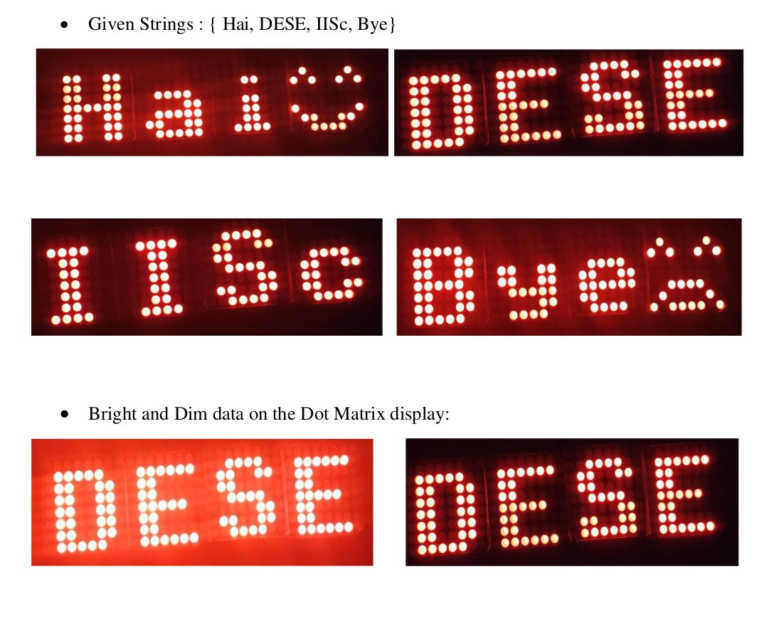
Given Strings : { Hai, DESE, IISc, Bye}
References
[1]MAX7219 datasheet
[2]TIVA C SERIES datasheet
*Datasheets are attached in project folder
Demo: Dot Matrix LED using Dma
code:dotmstrix code
Recent Comments