
DAC LTC1661 on EduARM4 Trainer Board
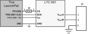
Fig:TM4C123 LaunchPad to LTC1661 Connection on EduARM4 Trainer Board
Note: Short 1 & 2 of J8 (EduARM4 Trainer Board)
Configuring SSI for SPI data transmission
After the GPIO configuration, we need to take the following steps to configure the SSI for the SPI protocol:
- Enable the clock to SSI module using RCGCSSI (SYSCTL_RCGCSSI_R).
- Disable the SSI via bit 1 of SSICR1 (SSIn_CR1_R) register before initialization.
- Set the Bit Rate with the SSICPSR (SSIn_CPSR_R) prescaler and SSICR0 (SSIn_CR0_R) control registers.
- Also select the SPI mode, phase, polarity, and data size in SSICR0 (SSIn_CR0_R) control register.
- Select the master mod in SSISCR1 (SSIn_CR1_R) register.
- Enable SSI using SSICR1 (SSIn_CR1_R) register.
- Assert slave select signal.
- Wait until the TNF flag (transmit FIFO not full) in SSISR (SSIn_SR_R status register) goes high, then load a byte of data into SSIDR (SSIn_DR_R data register) to be transmitted.
- Repeat step 8 above until all the data are in the FIFO.
- Wait until transmit is complete (transmit FIFO empty and SSI not busy).
- Deassert the slave select signal.
(where n = 0 to 3)
SPI Examples and Tasks
Sample Program
-
/* -
* Using SSI1 to send A to Z characters via SPI1 -
*/ -
#include <stdint.h> -
#include "inc/tm4c123gh6pm.h" -
void Init_SSI1(void);
-
void SSI1_Write(unsigned char data);
-
int main(void)
-
{ -
unsigned char i;
-
Init_SSI1();
-
for(;;) {
-
for (i = 'A'; i <= 'Z'; i++) {
-
SSI1_Write(i); /* write a character */
-
} -
} -
} -
void SSI1_Write(unsigned char data)
-
{ -
GPIO_PORTF_DATA_R &= ~0x04; /* assert SS low */
-
while((SSI1_SR_R & 2) == 0)
-
; /* wait until FIFO not full */
-
SSI1_DR_R = data; /* transmit high byte */
-
while(SSI1_SR_R & 0x10)
-
; /* wait until transmit complete */
-
GPIO_PORTF_DATA_R |= 0x04; /* keep SS idle high */
-
} -
void Init_SSI1(void)
-
{ -
SYSCTL_RCGCSSI_R |= 2; /* enable clock to SSI1 */
-
SYSCTL_RCGCGPIO_R |= 8; /* enable clock to GPIOD for SSI1 */
-
SYSCTL_RCGCGPIO_R |= 0x20; /* enable clock to GPIOF for slave select */
-
/* configure PORTD 3, 1 for SSI1 clock and Tx */ -
GPIO_PORTD_AMSEL_R &= ~0x09; /* disable analog for these pins */
-
GPIO_PORTD_DEN_R |= 0x09; /* and make them digital */
-
GPIO_PORTD_AFSEL_R |= 0x09; /* enable alternate function */
-
GPIO_PORTD_PCTL_R &= ~0x0000F00F; /* assign pins to SSI1 */
-
GPIO_PORTD_PCTL_R |= 0x00002002; /* assign pins to SSI1 */
-
/* configure PORTF 2 for slave select */ -
GPIO_PORTF_DEN_R |= 0x04; /* make the pin digital */
-
GPIO_PORTF_DIR_R |= 0x04; /* make the pin output */
-
GPIO_PORTF_DATA_R |= 0x04; /* keep SS idle high */
-
/* SPI Master, POL = 0, PHA = 0, clock = 4 MHz, 16 bit data */ -
SSI1_CR1_R = 0; /* disable SSI and make it master */
-
SSI1_CC_R = 0; /* use system clock */
-
SSI1_CPSR_R = 2; /* prescaler divided by 2 */
-
SSI1_CR0_R = 0x0007; /* 8 MHz SSI clock, SPI mode, 8 bit data */
-
SSI1_CR1_R |= 2; /* enable SSI1 */
-
}
Recent Comments