
The TM4C123GH6PM microcontroller contains two identical Analog-to-Digital Converter modules. These two modules, ADC0 and ADC1, provide 12-bit conversion precision and share the same 12 analog input channels. Each ADC module operates independently and can therefore execute different sample sequences, sample any of the analog input channels at any time, and generate different interrupts and triggers.
These two ADC modules provide the following features:
- 12 shared analog input channels
- 12-bit precision ADC
- Single-ended and differential-input configurations
- On-chip internal temperature sensor
- Maximum sample rate of one million samples/second (MSPS)
- Optional phase shift in sample time programmable
- Four programmable sample conversion sequencers from one to eight entries long, with corresponding conversion result FIFOs
- Five flexible trigger controls
- Software Trigger Controller (default)
- Timers
- Analog Comparators
- PWM
- GPIO
- Hardware averaging of up to 64 samples
- 2 Analog Comparators
ADC Programming with the Tiva TM4C123G
To program these two modules, ADC0 and ADC1, we need to understand some of the major registers. Figure 11.21 shows a simplified block diagram of a Tiva ADC module.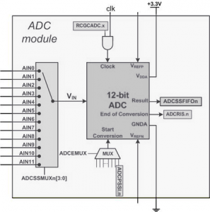
Enabling Clock to ADC
First thing we need to do is to enable the clock to the ADC0 or ADC1. Bit 0 and bit 1 of RCGCADC register are used to enable the clock to ADC0 and ADC1 modules, respectively. The RCGCADC is part of the System Control register and is located at base address of 0x400F.E000 with offset 0x638. That means, the RCGCADC is located at physical address of 0x400FE638 (0x400FE000 + 0x638 = 0x400FE638) in memory map. See Figure 11.22.
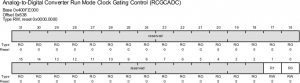
| bit | Name | Description |
|---|---|---|
| 0 | R0 | 0: ADC Module 0 is disabled, 1: Enable and provide a clock to ADC module 0 |
| 1 | R1 | 0: ADC Module 1 is disabled, 1: Enable and provide a clock to ADC module 1 |
The Sample Sequencer
The Sample Sequencer is a part of the ADC module that moves the conversion result of the ADC to one of the FIFOs. There are 4 Sample Sequencers. They are called SS3, SS2, SS1, and SS0. Each one of them is associated with a FIFO. The FIFOs have different sizes so the sample sequencers have different lengths of sequences. The longest sequence has 8 samples and the shortest has only one. Table 11.10 shows the relation between the sample sequencers and FIFO sizes.
| Sequencer | Number of Samples |
Depth of FIFO |
|---|---|---|
| SS0 | 8 | 8 |
| SS1 | 4 | 4 |
| SS2 | 4 | 4 |
| SS3 | 1 | 1 |
We will use the SS3 with a single sample. We use ADCACTSS (ADC Active Sample Sequencer) to enable the SS3. When bit 3 (ASEN3) is set to 1 the SS3 is enabled. We must disable the SS3 before configuring the sample sequencer so that no erroneous events occur during initialization. After the initialization is done, we must enable it to use it.
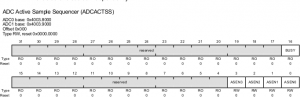
| Bit | Name | Description |
|---|---|---|
| 16 | BUSY | ADC Busy 0: ADC is idle, 1: ADC is busy |
| 3 | ASEN3 | ADC SS3 Enable 0: Sample Sequencer 3 is disabled, 1: Sample Sequencer 3 is enabled. |
| 2 | ASEN2 | ADC SS2 Enable 0: Sample Sequencer 2 is disabled, 1: Sample Sequencer 2 is enabled. |
| 1 | ASEN1 | ADC SS1 Enable 0: Sample Sequencer 1 is disabled, 1: Sample Sequencer 1 is enabled. |
| 0 | ASEN0 | ADC SS0 Enable 0: Sample Sequencer 0 is disabled, 1: Sample Sequencer 0 is enabled. |
Start Conversion trigger options
There are many start-conversion (trigger) options. Among them are using Timer, PWM, Analog Comparator, External signal from GPIO, and Software. The selection of Trigger for SS3 is done via the bits 15-12 of ADCEMUX register. The default is Software and that is what we use in this section.
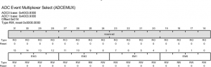
EMx bits select the trigger source for Sample Sequencer x. By default the field is 0x0 which means the ADC conversion begins when the SSn bit of the ADCPSSI register is set by software. The following table shows the available choices for trigger.
| EMx Value | Trigger source |
|---|---|
| 0x0 | Processor (default) |
| 0x1 | Analog Comparator 0 |
| 0x2 | Analog Comparator 1 |
| 0x3 | reserved |
| 0x4 | External (GPIO Pins) |
| 0x5 | Timer |
| 0x6 | PWM Generator 0 |
| 0x7 | PWM Generator 1 |
| 0x8 | PWM Generator 2 |
| 0x9 | PWM Generator 3 |
| 0xF | Always (continuously sample) |
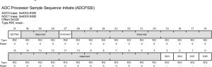
After we select the software option bit (which is the default) in the ADCEMUX, we must use bit D3 of ADCPSSI register to start a conversion every time we want a new reading from the ADC input channel.
| SSx Value | Trigger source |
|---|---|
| 0 | No Effect |
| 1 | Begin sampling on sample sequence x |
Notice that we can trigger the SS3 option only if we have enabled the SS3 in the ADCACTSS register.
Choosing Vin input channel
The channel selection is done through the ADCSSMUXn (n=0, 1, 2, 3) registers. For the SS3, the ADCSSMUX3 is used. Since SS3 only handles single conversion, bits 3 – 0 are used to specify the analog channel to be converted. The number of available channels in the TI Tiva TM4C123G varies among the family members. In the case of TI Tiva TM4C123GH6PM, there are 12 channels. They are designated as AIN0 (analog input 0) to AIN11 (analog input 11). Their designated pins are shown in Table 11.12.
| Pin Name |
Description | Pin | Pin Number |
|---|---|---|---|
| AIN0 | ADC input 0 | PE3 | 6 |
| AIN1 | ADC input 1 | PE2 | 7 |
| AIN2 | ADC input 2 | PE1 | 8 |
| AIN3 | ADC input 3 | PE0 | 9 |
| AIN4 | ADC input 4 | PD3 | 64 |
| AIN5 | ADC input 5 | PD2 | 63 |
| AIN6 | ADC input 6 | PD1 | 62 |
| AIN7 | ADC input 7 | PD0 | 61 |
| AIN8 | ADC input 8 | PE5 | 60 |
| AIN9 | ADC input 9 | PE4 | 59 |
| AIN10 | ADC input 10 | PB4 | 58 |
| AIN11 | ADC input 11 | PB5 | 57 |
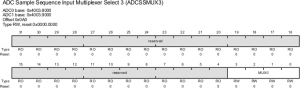
| bit | Name | Desription |
|---|---|---|
| 0-3 | MUX0 | Sample Input Select |
Polling or interrupt
The end-of-conversion is indicated by a flag bit in the ADCRIS (ADC Raw Interrupt) register. Upon the completion of conversion for the SS3, the D3 bit (INR3) flag goes high. By polling this flag, we know if the conversion is complete and we can read the value in ADCSSFIFO3 register. We can also use an interrupt to inform us that the conversion is complete but that will require us to set up the interrupt mask ADCIM. By default, the interrupts are not enabled.
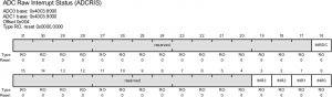
| bit | Name | Discription |
|---|---|---|
| 0 | INR0 | SSO Raw Interrupt Status 0:An interrupt has not occured 1: A sample has completed conversion and respective ADCSSCTL0 len bit is set, enabling a raw interrupt. Note: This bit is cleared by writing a 1 to the IN0 bit in the ADCISC register. |
| 1 | INR1 | SS1 Raw Interrupt Status |
| 2 | INR2 | SS2 Raw Interrupt Status |
| 3 | INR3 | SS3 Raw Interrupt Status |
| 16 | INRDC | Digital Comparator Raw Interrupt Status 0: All bits in the ADCDCISC register are clear. 1: At least one bit in the ADCDCISC register is set, meaning that a digital comparator interrupt has occurred. |
ADC Data result
Upon the completion of conversion, the binary result is placed in the ADCSSFIFOn register. Since we are using SS3, we need to read the result from ADCSSFIFO3 register. This is 32-bit register but only the lower 12 bits are used.
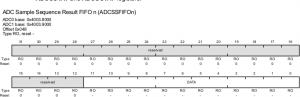
| bit | Name | Description |
|---|---|---|
| 0-11 | DATA | Conversion Result Data |
Clearing end-of-conversion flag
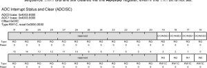
After reading the data from the ADCSSFIFOx register, we must clear the INR3 flag bit in ADCRIS register so that we may detect another conversion complete. The raw interrupt flag in ADCRIS is cleared by writing to ADCISC (ADC Interrupt Status and Clear) register. By writing a 1 to bit 3 (IN3 bit) of ADCISC, the interrupt flag is cleared and we can do another conversion again.
| bit | Name | Description |
|---|---|---|
| 0-3 | INx | SSx Interrupt Status and Clear 0: No Interrupt has occurred or the interrupt is masked 1: A sample has completed conversion (the INRx bit in the ADCRIS register is set) and the MASKx bit in the ADCIM register is set, providing an interrupt to the interrupt controller. Note: This bit is cleared by writing a 1. Clearing the bit also clears the INRx bit in the ADCRIS register. |
| 16 to 19 |
DCINSSx | Digital Comparator Interrupt Status on SSx 0:No Interrupt has occurred or the interrupt is masked 1: Both the INRDC bit in the ADCRIS register and the DCONSSx bit in the ADCIM register are set providing an interrupt to the interrupt controller. Note: This bit is cleared by writing a 1. Clearing the bit also clears the INRDC bit in the ADCRIS register. |
Differential versus Single-Ended
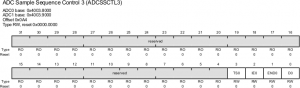
In some applications, our interest is in the differences between two analog signal voltages (the differential voltages). Rather than converting two channels and calculate the differences between them, the Tiva TM4C123G has the option of converting the differential voltages of two analog channels. The bit 0 of ADCSSCTL3 (ADC Sample sequence Control 3) register allows us to enable the differential option. Upon Reset, the default is the single-ended input. The pairing of the analog inputs for differential is hardwired. Table 11.13 shows the pairing of the ADC input channels for differential option.
| Differential Pair | Analog Inputs |
|---|---|
| 0 | 0 and 1 |
| 1 | 2 and 3 |
| 2 | 4 and 5 |
| 3 | 6 and 7 |
| 4 | 8 and 9 |
| 5 | 10 and 11 |
The other bits in ADCSSCTL3 register are bit 1 (END0), bit 2 (IE0), and bit 3 (TS) bits. On some of the ADC inputs, we have an internal temperature sensor embedded into the chip. Making bit 3 = 1, reads the temperature sensor value inside the chip itself. Since we are using one sample in the SSE3, we must enable the bit 1 (END0) to let ADC know that first sample is the only sample and there is no sample coming after that. Bit 2 (IE0) is the Interrupt enable. It causes the raw interrupt flag to set when this sample conversion is completed. However, in order to redirect the end-of-conversion to the NVIC interrupt controller, we must also enable the bit in ADCIM register, as we will see soon. It must be noted, even if we do not want to use interrupt, we must still set IE0 = 1, in order to post the raw interrupt flag for polling the conversion complete.
| bit | Name | Description |
|---|---|---|
| 0 | D0 | Sample Differential Input Select 0: The analog inputs are not differentially sampled 1: The analog inputs are differentially sampled. The corresponding ADCSSMUX nibble must be set to the pair number “i”, where the paired inputs are 2i and 2i+1. Note: Because the temperature sensor doesn’t have a differential option this bit must not be set when the TS0 bit is set. |
| 1 | END0 | End of Sequence: This bit must be set before initiating a single sample sequence. 0: Sampling and conversion continues 1: This is the end of the sequence. |
| 2 | IE0 | Sample Interrupt Enable 0: The raw interrupt is not asserted to the interrupt controller 1: The raw interrupt signal (INR0 bit) is asserted at the end of this sample’s conversion. If the MASK0 bit in the ADCIM register is set, the interrupt is promoted to the interrupt controller. It is legal to have multiple samples with in a sequence generate interrupts. |
| 3 | TS0 | 1st Sample Temperature Sensor Select 0: The input pin specified by the ADCSSMUXn register is read during the first sample of the sample sequence. 1: The temperature sensor is read during the first sample sequence. |
Masking interrupt for SS3
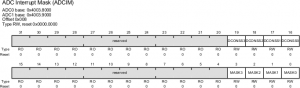
Since we are using polling for the end-of-conversion, we must mask the interrupt option for the SS3 to prevent it from interrupting us via NVIC. This is done with bit 3 of ADCIM (ADC Interrupt Mask) register. Upon Reset, the default for the bit 3 (MASK3) is 0. With the MASK3 = 0, it disables the interrupt and we will leave it like that. However, if we like to handle end-of-conversion by interrupt, we need to set this bit to 1 and write an interrupt handler to read the conversion result.
| bit | Name | Description |
|---|---|---|
| 0-3 | MASKx | SSx Interrupt Mask 0: The Status of Sample Sequencer x doesn’t affect the SSx Interrupt Status. 1. The raw interrupt signal from Sample Sequencer x (ADCRIS register INRx bit) is sent to the interrupt controller. |
| 16 to 19 |
DCONSSx | Digital Comparator Interrupt on SSx 0: The status of the digital comparators doesn’t affect the SSx interrupt status. 1: The raw Interrupt signal from digital comparators (INRDC bit in the ADCRIS register) is sent to the interrupt controller on the SSx interrupt line. |
Vref in Tiva LaunchPad
In the TI ARM Tiva chip series, the pin for Vref (+) is called VDDA (VDD analog) and Vref (-) pin is called GNDA (Ground Analog). In the TI Tiva LaunchPad, the VDDA pin is connected to 3.3V, the same supply voltage as the digital part of the chip.
Even if we connect the VDDA to a separate power source other than the VDD of the chip, it cannot go beyond the VDD voltage. With Vref=3.3V, we have the step size of 3.3V / 4096 = 0.8057 mV since the ADC resolution is 12 bits.
Operational Procedure for ADC
Each ADC module contains four sample sequencers, SS0 – SS3. Each sample can be obtained from different input sources (different channels). These sample sequencers are under the control of some control registers in the Control/Status block. The operational procedure of each ADC module includes:
- Each ADC module must be clocked by configuring the ADC Clock Configuration (ADCCC) register before it works since all ADC modules share the same clock source to facilitate the synchronization of data samples between conversion units.
- Before the ADC can start its conversion, the sample sequencers must be configured by related registers in each sample sequencer block, such as ADC Sample Sequence Input Multiplexer Select n (ADCSSMUXn) and ADC Sample Sequence Control n (ADCSSCTLn) registers.
- Then the sample sequencers must be enabled by configuring the ADC Active Sample Sequencer (ADCACTSS) register. If multiple triggering events were used, the ADC Sample Sequencer Priority (ADCSSPRI) register must also be configured.
- The trigger source or trigger event must be determined by configuring the ADC Event Multiplexer Select (ADCEMUX) register, and the sampling process must be initiated by setting up the ADC Processor Sample Sequence Initiate (ADCPSSI) register.
- Optionally, one can use the ADC Peripheral Property (ADCPP) register to set up the resolution, include the temperature sensor, and set the ADC sample rate. Generally, you do not need to touch this register and only use the default settings of this register.
- The ADC Trigger Source Select (ADCTSSEL) register is used to select a PWM generator as the trigger source when the PWM generator is used.
- After the analog input channel and sample property have been determined by ADCSSMUXn, ADCSSCTLn registers, the ADC conversion starts. After the ADC conversion is complete, the conversion results can be obtained from the ADC Sample Sequence Result FIFO (ADCSSFIFOn) registers.
- If interrupts are used for any ADC conversion, some registers in the Interrupt Control block should also be configured.
The Hardware Averager is used to make the ADC conversion results smoother by averaging some continuous samples. The Digital Comparator is used to compare the ADC conversion results with some predefined values to monitor and control the external signals.
Recent Comments