
Configuring GPIO for ADC input
In using ADC, we must also configure the GPIO pins to allow the connection of an analog signal through the input pin. In this regard, it is the same as all other peripherals. The steps are as follows:
- Enable the clock to GPIO pin by using RCGCGPIO.
- Set the GPIOAFSEL (GPIO alternate function) bit for ADC input pin to 1.
- Configure AINx signal to be used as analog input by clearing the bit in the GPIODEN (GPIO Digital enable) register.
- Disable the Analog isolation circuit for ADC input pins by writing a 1 to the GPIOAMSEL register.
Configuring ADC and reading ADC channel
After the GPIO configuration, we need to take the following steps to configure the ADC for Sample Sequencer 3 (SS3):
- Enable the clock to ADC0 or ADC1 modules using RCGCADC register of System Registers.
- The SYSCTL_RCGCADC_R |= 3 will enable the clock to both ADC0 and ADC1 modules. For ADC0 module use SYSCTL_RCGCADC_R |= 1
- Disable the Sample Sequencer using the ADCACTSS register before changing the configuration of the sequencer.
- ADC0_ACTSS_R &= ~8 disables the SS3.
- Choose the software trigger using the ADCEMUX register.
- Use ADC0_EMUX_R &= ~0xF000 for software trigger.
- Select the ADC input channel using the ADCSSMUXn register. In the case of SS3 we use the ADCSSMUX3.
- For example, The ADC0_SSMUX3_R = 0 selects AIN0 channel on pin PE3.
- Select the single-ended option, one-conversion per sample, and raw interrupt bit for end-of-conversion using the ADCSSCTL3 register.
- Use ADC0_SSCTL3_R |= 6 for single-ended, one-conversion, and raw interrupt.
- Enable the Sample Sequencer SS3 using ADCACTSS register.
- ADC0_ACTSS_R |= 8 enables the SS3.
- Use ADCPSSI register to start a new conversion.
- Use ADC0_PSSI_R |= 8 to start a conversion by Sample Sequencer 3.
- Keep monitoring the end-of-conversion INR3 flag in ADCRIS (ADC0_RIS_R) register.
- When the INR3 goes HIGH, read the ADC result from the ADCSSFIFO3 (ADC0_SSFIFO3_R) and save it.
- After reading the ADC result in step 9, clear the INR3 flag in ADCRIS register to allow for the next conversion.
- To clear INR3 flag, write to ADCICS register with ADC0_ISC_R = 8.
- Repeat steps 7 through 10 for the next conversion.
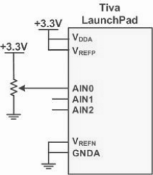
Figure 11.31: ADC Connection for the following Program
Source Code
-
/* A to D conversion -
* -
* This program converts the analog input from AIN0 (J3.9 of LaunchPad) -
* using sample sequencer 3 and software trigger continuously. -
* -
* Note: AIN0 channel is on PE3 pin. -
* -
*/ -
#include <stdint.h> -
#include "inc/tm4c123gh6pm.h" -
int main(void)
-
{ -
volatile int result;
-
/* enable clocks */ -
SYSCTL_RCGCGPIO_R |= 0x10; /* enable clock to PE (AIN0 is on PE3) */
-
SYSCTL_RCGCADC_R |= 1; /* enable clock to ADC0 */
-
/* initialize PE3 for AIN0 input */ -
GPIO_PORTE_AFSEL_R |= 8; /* enable alternate function */
-
GPIO_PORTE_DEN_R &= ~8; /* disable digital function */
-
GPIO_PORTE_AMSEL_R |= 8; /* enable analog function */
-
/* initialize ADC0 */ -
ADC0_ACTSS_R &= ~8; /* disable SS3 during configuration */
-
ADC0_EMUX_R &= ~0xF000; /* software trigger conversion */
-
ADC0_SSMUX3_R = 0; /* get input from channel 0 */
-
ADC0_SSCTL3_R |= 6; /* take one sample at a time, set flag at 1st sample */
-
ADC0_ACTSS_R |= 8; /* enable ADC0 sequencer 3 */
-
while(1) {
-
ADC0_PSSI_R |= 8; /* start a conversion sequence 3 */
-
while((ADC0_RIS_R & 8) == 0)
-
; /* wait for conversion complete */
-
result = ADC0_SSFIFO3_R; /* read conversion result */
-
ADC0_ISC_R = 8; /* clear completion flag */
-
} -
}
Note
- Short 3 & 4 of J7 on the EduARM4 Trainer Board
- To change the input voltage to the ADC, Vary the RV2 potentiometer.
Recent Comments