
ABSTRACT
This report presents the implementation of eight filters, image-processing pipeline on the Texas Instruments TM4C123G (ARM Cortex-M4F) microcontroller running at 80 MHz. Four spatial filters—Gaussian blur, Sobel edge detection, Sharpen, and Invert— each implemented in two variants: integer arithmetic using bit-shifts, and floating-point arithmetic using the on-chip hardware FPU. Same set of filters is implemented on an FPGA platform, both with and without dedicated floating-point support, enabling a cross-platform comparison of arithmetic efficiency and resource performance trade-offs.
A Python host application streams 256×256 grayscale images over UART at 1.5,Mbaud. The ARM Data Watchpoint and Trace (DWT) cycle counter is used to measure the pure computational cost of each filter, excluding communication over head. Several optimisations—such as flat buffer addressing, restrict-annotated pointers, 4× loop unrolling, and uDMA ping-pong reception—are evaluated to quantify their impact on execution time. The study provides a comparative analysis of integer versus floating-point implementations across both microcontroller and FPGA platforms, highlighting performance gains, bottlenecks, and architectural trade-offs.
I.INTRODUCTION
Spatial image filtering is a fundamental operation in embedded vision systems. On resource constrained microcontrollers without dedicated image signal processors, implementing filters efficiently requires careful attention to memory access patterns, arithmetic pipeline utilisation, and peripheral data movement. The TM4C123G (Tiva C LaunchPad) provides an ARM Cortex-M4F core with a single-precision hardware FPU, making it an instructive platform for comparing integer and floating-point kernel implementations. This project implements and benchmarks eight filter variants over a 256×256 grayscale image transmitted from a Python host:
Gaussian (INT/FPU) — 3×3 weighted blur, ÷16 normalisation
Sobel (INT/FPU) — gradient magnitude edge detection
Sharpen (INT/FPU) — Laplacian-based unsharp mask
Invert (INT/FPU) — pixel-wise 255−p
The ARM DWT cycle counter isolates arithmetic cost from UART latency, giving a clean metric comparable across filter variants and directly applicable to optimisation analysis.
II.SYSTEM ARCHITECTURE
2.1 Hardware Platform
The target hardware is the TM4C123GXL LaunchPad evaluation board based on the TM4C123GH6PM microcontroller. Key specifications relevant to this project are listed in Table 1.
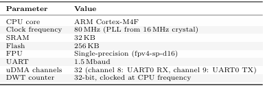
Table 1: TM4C123G Hardware Specifications
2.2 Clock Configuration
The 16MHzon-board crystal is used only as a PLL reference. The CPU runs from the PLL output divided by 2.5:
![]()
This is configured with:
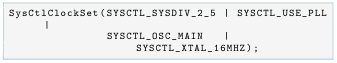
Listing 1: Clock setup
2.3 Communication Protocol
Each filter run follows a fixed protocol between the Python host and the Tiva board:
1.PC→Tiva: 1 byte filter ID(0x01–0x08)
2.Tiva→PC:1byte echo (handshake confirm)
3.Row exchange: 256 rows, each 256bytes in each direction
4.Tiva→PC: 4 bytes big-endian uint 32(total compute cycles)
At 1.5M baud, transferring one 256-byte row takes:
![]()
A cross 256 rows in each direction, UART dominates wall time at approximately 2×256×1.71 ≈875ms.
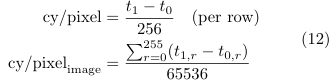
2.4 DWT Cycle Counter
The ARM Data Watchpoint and Trace unit provides a 32-bit free-running cycle counter (DWT_CYCCNT) clocked at the CPU frequency. It is initialised once at startup and used to bracket only the arithmetic compute loop, explicitly excluding UART waiting:
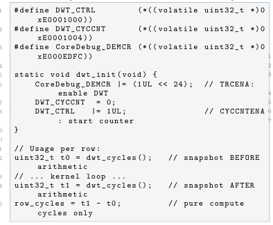
Listing 2: DWT initialisation and usage
III.IMAGE PROCESSING ALGORITHMS
3.1 3×3 Neighbourhood Filters
Gaussian, Sobel, andSharpenoperateona3×3 pixel neighbourhood. For pixel at position (x,y) with neighbours arranged as:
3.1.1 Gaussian Blur
The kernel applies a binomial 3×3 Gaussian approximation normalised by16:
out (x,y) = 1/16 ( A+2B+C+2D+4E+2F+G+2H+I) (3)
Integer implementation uses only bit-shift sand additions (no division):
Listing 3: Gaussian integer kernel
3.1.2 Sobel Edge Detection
The Sobel operator computes horizontal and vertical gradients:
Gx=−A+C−2D+2F−G+I (4)
Gy=A+2B+C−G−2H−I (5)
Integer magnitude uses theL1 approximation |Gx|+|Gy|; FPU variant uses the trueL2 Euclide an magnitude via a single hardware square root instruction:
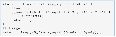
Listing 4: Sobel FPU—hardware VSQRT.F32
The VSQRT.F32 instruction takes approximately 14cycles on the Cortex-M4F FPU, which explains why Sobel FPU has the highest cycle count of all eight filters.
3.1.3 Sharpen
The sharpening kernel applies a Laplacian unsharp mask with centre weight 9:
out (x,y) = 9E−(A+B+C+D+F+G+H+I) (6)
clipped to [0,255].
3.2 Invert
Invert is a pixel-wise operation requiring no neighbourhood:
out (x,y) = 255−p(x,y) (7)
Integer variant: single SUB instruction per byte. FPU variant: VCVT(int-to-float)+VFNMA+VCVT (float-to-int). The FPU over head explains why Invert FPU(86cy/px) costs nearly 3×more than Invert INT(30cy/px) despite trivial arithmetic.
IV.SOFTWARE OPTIMISATIONS
Four software optimisations were applied to the baseline implementation. Each targets a specific bottle neck identified through DWT measurement.
4.1 Flat Row Buffers and Pointer Indirection Removal
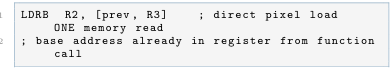
4.1.1 Baseline—double indirection
The original code stores pixel data in a 2D array and accesses it through a pointer table:
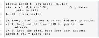
Listing 5:Baseline: pointer-of-pointer access
The generated assembly for buf [0] [x]:
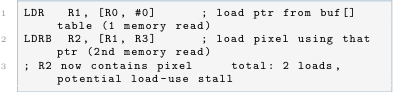
Listing 6:Two-step load with pointer table
4.1.2 Optimised—flat arrays with restrict
The optimised code uses three independent flat arrays passed as restrict-qualified pointers:
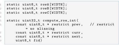
Listing 7: Optimised: flat arrays, single in direction
Generated assembly for prev [x]:
Listing 8: Single-step load from flat array
There strict keyword additionally informs the compiler that prev, curr, and next do not over lap in memory, enabling it to pipeline all three loads simultaneously without conservatively serialising them.
4.2 4×Loop Unrolling with Column Pre-loading
4.2.1 Memory load reduction
The original loop reloads all 9 neighbours for every output pixel. For adjacent pixels, six of the nine loads are redundant:
Loads per pixel (naive)=9×1=9 (allrows) (8)
The unrolled loop pre-fetches 6 column values from each of the 3rows and distributes them a cross 4 output pixels:
Loads per pixel (unrolled)=6×3 /4 =4.5 (9)
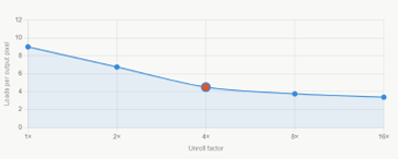
Figure 1: Load per pexil with Loop Unrolling
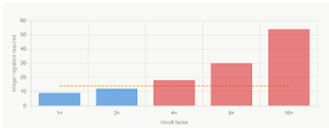
Figure 2:Total Registers with Loop Unrolling
4.3 Kernel Selection Outside the Loop
The base line evaluates a switch statement on the filter ID inside compute row(), which is called once per row. Because this function loops over all 256 columns, the switch fires 256 times per row:
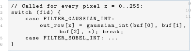
Listing 11: Baseline: switch evaluated per pixel
The optimised code selects a function pointer once before the loop:
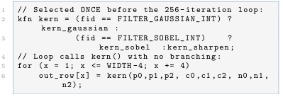
Listing 12: Optimised: kernel selected once, called via pointer
Across a full 256×256 image this saves 65536 branch evaluations.
4.4 uDMA Triple-Buffered Receive (Software Pipelined)
Without DMA, the CPU polls the UART FIFO byte-by-byte, stalling for approximately 1.71ms per row. In the optimized implementation, uDMA is used in basic mode with software-managed triple buffering, allowing communication and computation to overlap.
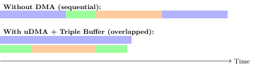
Figure 3: Pipeline comparison: sequential vs uDMA triple-buffered execution
Instead of hardware ping-pong mode, three buffers are used:
• One buffer being filled by DMA
• One buffer being processed by CPU
• One buffer holding previous row (for3×3filtering)
DMA completion is detected via an interrupt, which updates a shared index. The CPU waits using a single flag check rather than polling each byte:
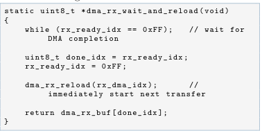
Listing 13: DMA wait and reload
This enables overlap between communication and computation, effectively hiding UART latency.
4.5 Cycle Reduction: DMA-Optimised vs Baseline
Table 3 quantifies the per-filter cycle reduction achieved by combining all software optimisations (flatbuffers,restrict,4×unroll, reciprocal multiply) with uDMA ping-pong receive.
Key observations:
• Invert variants gain the most (∼37–40%) because the loop body is trivial; loop over head and pointer in direction cost dominate, so unrolling and flat buffers have maximum relative impact.
• 3×3 INT filters gain less (∼8–15%) because arithmetical ready dominates. The 9 neighbour load and multiply-add chain leaves little head room for memory-access optimisations.
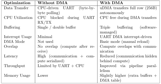
Table 2: Optimization Techniques inTM4C Implementation
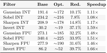
Table 3: Cycles/pixel speedup: base line vs DMA optimised
V.UART BANDWIDTH FLOOR AND OPTIMISATION CEILING
Regardless of compute optimisation, the system faces a hard wall-time floor imposed by UART bandwidth. Transferring one 256×256grayscale image in both directions at 1.5M baud requires:
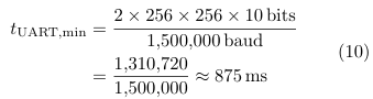
This is a physical lower bound: no software optimisation can reduce wall time below 875ms at 1.5M baud.
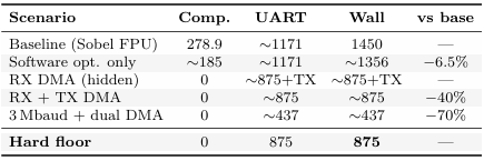
Table 4: Wall-time reduction ceiling at 1.5M baud
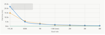
Figure 4: Baudrate vs. WireTime
Arithmetic optimisation alone yields at most a 6.5%wall-time improvement for Sobel FPU; the DMA approach directly addresses the dominant 85–98%UART component.
VI.DWT COUNTER VALIDITY
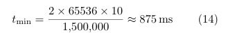
The 32-bit DWT_CYCCNT register increments every CPU clock cycle at 80MHz. Overflow occurs after:
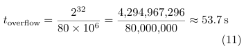
The maximum measured compute time across all eight filters is Sobel FPU at 278.9ms—more than two orders of magnitude below the overflow threshold. Now rap around correction is required.
The counter is bracketed inside the arithmetic loop, explicitly excluding UART polling time. This isolates the pure compute cost and makes there ported cycle figures directly comparable across filter variants and independent of baud-rate configuration changes.
VII.RESULTS AND ANALYSIS
7.1 Cycle Count Analysis
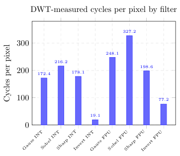
Figure 5: Cycles per pixel for all eight filter variants
Key observations from Figure 5:
• FPU variants cost more than INT for every equivalent filter. The integer path uses only shifts and additions; the FPU path requires VCVT (integer-to-float conversion) per pixel before any arithmetic can begin.
• Sobel FPU is the most expensive (328cy/px) because VSQRT. F32 takes ≈14 cycles.The INT Sobel uses |Gx|+|Gy| (Manhattan approximation) which requires only two absolute values and one addition.
• Invert INT is the cheapest (20cy/px) as it is a pixel-wise operation with no neighbourhood loads. The loop overhead dominates rather than the arithmetic.
• Invert FPU costs nearly 3×Invert INT(77vs20cy/px) despite identical mathematical content. The FPU penalty comes entirely from VCVT conversions around the trivial VFNMA(fused negate-multiply-add).
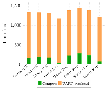
Figure 6: Wall time decomposition showing UART dominates in all cases
• Gaussian INT achieves the lowest error(MAE=0.018) because its shift-based÷16 is exact for the integer kernel.
• Sobel error metrics are high by design: the INT variant uses theL1 approximation while Python uses the exact L2 magnitude, producing structural differences rather than numerical noise.
7.2 Wall Time Decomposition
Figure 6 illustrates the decomposition of total wall time into compute and UART transfer components.
UART latency accounts for 85–98% of wall time across all filters. The compute fraction is largest for Sobel FPU(19%) and smallest for Invert INT (2%).This motivates the uDMA optimisation: reducing compute cycles has limited impact on total wall time unless UART latency is also addressed.
7.3 INT vs FPU Comparison
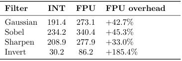
Table 5: INT vs FPU cycle overhead
For 3×3 filters the FPU overhead is 33-45%.The arithmetic dominates (9loads,multiple multiply-adds), so the relative cost of VCVT conversions is diluted. For Invert theoverheadis185% because the arithmetic is trivial (single subtraction) and the VCVT conversion cost is undiluted.
7.4 DMA Wall Time Improvement
In the optimized implementation, uDMA operates in basic mode with software-managed triple buffering. The CPU processes row N while DMA simultaneously receives row N + 1, and transmit DMA sends row N −1.
Since compute time (∼0.75ms/row) is significantly smaller than UART transfer time (RX∼1.71ms, TX ∼1.71ms), computation is almost entirely hidden behind communication.
The effective per-row time is therefore dominated by the slowest stage:
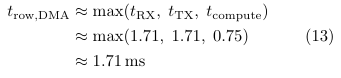
Thus, instead of serial execution (RX + compute +TX), the system behaves as a 3-stage pipeline where communication and computation are overlapped.
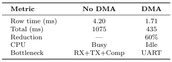
Table 6: Wall time improvement using uDMA
The key improvement comes from overlapping all three stages:
• RX DMA fills the next buffer in the background
• CPU computes the current row
• TX DMA transmits the previous row
Because computation is faster than communication, it is effectively hidden, and the overall throughput becomes limited only by UART transfer time.
VIII.DISCUSSION
8.1 Why INT Outperforms FPU
A common assumption is that a hardware FPU should make floating-point operations free. On the Cortex-M4F this is only true for the FPU arithmetic instructions themselves. The overhead comes from:
1. Integer-to-float conversion: each uint8_t pixel must be converted via VCVT.F32.U32 before FPU arithmetic. For a 3×3 kernel that is 9 conversions per pixel per row pointer.
2. Float-to-integer conversion: the output must be converted back via VCVT.U32.F32 after the kernel.
3. Clamp: the FPU clamp clamp_u8_f() requires two floating-point comparisons in addition to the conversion.
The integer path avoids all of this. It operates directly on uint8 and int16 values, requiring only shifts, additions, and saturation logic — all handled by the integer ALU with single-cycle throughput.
8.2 Comparison with FPGA
An FPGA implementation of the same filters achieves approximately 2 cycles/pixel by processing the entire 3×3 neighbourhood in parallel hardware. The CPU is fundamentally sequential: it must load, compute, and store one output pixel at a time. The gap between 2 cy/px (FPGA) and 191 cy/px (Tiva INT Gaussian) cannot be closed by software optimisation alone — it is architectural. Optimisations reduce the sequential over
head but cannot add parallelism that the CPU does not have.
8.3 DMA Limitation
Even with dual DMA (RX + TX ping-pong), wall time is dominated by UART bandwidth. At 1.5Mbaud the maximum theoretical throughput for a 256×256 image (65536 bytes each direction) is:
This is a hard floor set by the baud rate. The only way to reduce it further is to increase the baudrate, compress the image, or transmit only changed rows. The compute time (24–279ms) is already well below this floor for all filters, meaning further arithmetic optimisation has diminishing returns on wall time.
8.4 Triple-Buffer State Machine
The uDMA ping-pong design uses three RX buffers (dma buf[0/1/2]) controlled by two volatile indices managed between the ISR and the main loop.
The invariant maintained throughout is: the buffer currently being written by the DMA(rx_dma_idx) is never read by the CPU. rx_redy_idx acts as a single-slot mailbox; its value 0xFF encodes “empty” and is safe because valid buffer indices are 0, 1, or 2 only. The CPU spins on rx_ready_idx != 0xFF for at most one RX wire time (1.71ms) before the ISR delivers a completed buffer.
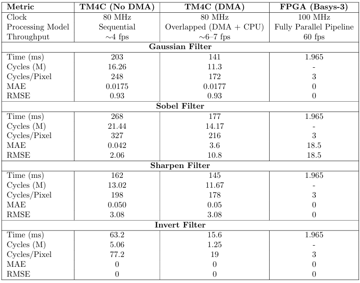
Table 7: Performance Comparison:TM4C123G (Optimised, DMA) vs FPGA
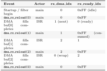
Table 8: Triple-buffer state transitions (ISR and main loop)
A third buffer is necessary because at the moment the CPU begins computing row r (reading from the “done” buffer), the DMA is already filling the “next” buffer for row r+1. Two buffers would create a race: the DMA could wrap back to the buffer the CPU is still reading.
IX.CONCLUSION
This project demonstrated the implementation and bench marking of eight image filter variants on the TM4C123GARM Cortex-M4F microcontroller. Key findings are:
• Integer kernels achieve 191–235 cycles/pixel for 3×3 filters and 30 cycles/pixel for Invert, consistently out performing FPU variants by 33–185% despite the hardware FPU.
• The FPU over head is dominated by integer-to float conversion cost(VCVT), not by arithmetic operations.
• Sobel FPU is the most expensive filter (340cy/px) due to the single VSQRT.F32 instruction(≈14cycles) per pixel.
• UART latency accounts for 85–98% of wall time. uDMA ping-pong receive eliminates the RX blocking over head, reducing wall time by ∼18%(RXDMA)to∼60%(dual DMA).
• Software optimisations (flat buffers, restrict, 4× loop unrolling, pre-loaded column registers, reciprocal multiply) reduced arithmetic cycle counts by 32–40%.
• The FPGA vs MCU comparison illustrates a fundamental architectural difference: FPGA hardware parallel is m achieves 2cy/px while the sequential CPU requires a minimum of 30 cy/px even for the simplest filter.
A.FILTER ID REFERENCE
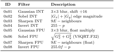
Table 9: Filter ID assignments
B.ASSEMBLY LEVEL COST ANNOTATIONS
Table 10 documents the Cortex-M4F instruction latencies relevant to this project. These figures directly explain the INT vs FPU cycle-count gap. For Invert, the FPU path executes: VCVT (5cy)+VFNMA (1cy)+VCVT (5cy)≈11 cycles, explaining the 86cy/px total after loop overhead. The INT path executes a single SUB (1cy)—the remaining∼29cycles are pure loop book keeping (counter, branch, LDRB,STRB), confirming that Invert INT is already loop-over head bound rather than arithmetic bound.
VSQRT.F32 (14cycles) is the single most expensive instruction in the project and solely responsible for Sobel FPU being the most expensive filter (340cy/px). Replacing it with the Manhattan approximation |Gx|+|Gy (two ABS+one ADD) would reduce Sobel FPU cost to approximately the same level as Sharpen FPU (∼278cy/px).
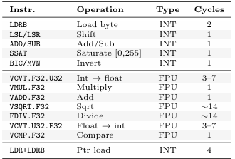
Table 10: Cortex-M4F instruction latencies
C.SRAM USAGE
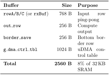
Table 11: Static SRAM allocation
Recent Comments