
To provide an easy way to turn off the PWM output, each PWM generator has an enable register PWMENABLE. Since many of the PWM registers are shared, this allows us to disable a given PWM signal from going to the output pin without disturbing the rest of the PWMs. The lower 8 bits of the PWMENABLE register are used for enabling or disabling the PWM0 to PWM7. When the bit is enabled, the signal generated by the PWM generator is connected to the output pin. When the bit is disabled, there will be no output but the PWM generator still runs without any change.
There are total of 8 PWM pins supported by each PWM module. The PWM pins for each of PWM module are designated as PWM0, PWM1, PWM2, …, PWM7 as shown in Figure 14.1.
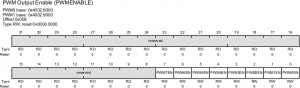
We use PWM0_ENABLE_R and PWM1_ENABLE_R to control the outputs of PWM0 and PWM1, respectively. The offset addresses are the same except the base address is different, as we mentioned earlier. See Figure 16.1.
| bit | Name | Description |
|---|---|---|
| 0 | PWM0EN | MnPWM0 Output Enable 0: The MnPWM0 signal has zero value. 1: The generated pwm signal is passed to the MnPWM0 pin. |
| 1 | PWM1EN | MnPWM1 Output Enable 0: The MnPWMx signal has zero value. 1: The generated pwm signal is passed to the MnPWM1 pin |
The role of the PWMENABLE register is shown in the PWM Output Control part of Figure 16.1.
Selecting alternate function for PWMx pin
Upon reset, the GPIOAFSEL register has all 0s meaning the I/O pins are used as simple I/O. To use the alternate function, we first must set to 1 the bit in the AFSEL register for that pin. For example, for the PB6, we need to write 0x40 (01000000 in binary) to GPIO_PORTB_AFSL register. See Tables 16.1 and 16.2. After that, the GPIOPCTL register must be configured for the desired function, as shown in Tables 16.1 and 16.2. The alternate functions for each I/O pin are listed in Table 23-5 of TI Tiva LaunchPad manual. Tables 16.1 through 16.2 provide the summary for the M0PWMx and M1PWMx pins. See Example 16.1.
| M0PWMx | PIN | Value for GPIOAFSL register | Value for GPIOPCTL register |
|---|---|---|---|
| M0PWM0 | PB6 | GPIO_PORTB_AFSEL_R = 0x40 | GPIO_PORTB_PCTL_R=0x04000000 |
| M0PWM1 | PB7 | GPIO_PORTB_AFSEL_R = 0x80 | GPIO_PORTB_PCTL_R=0x40000000 |
| M0PWM2 | PB4 | GPIO_PORTB_AFSEL_R = 0x10 | GPIO_PORTB_PCTL_R=0x00040000 |
| M0PWM3 | PB5 | GPIO_PORTB_AFSEL_R = 0x20 | GPIO_PORTB_PCTL_R=0x00400000 |
| M0PWM4 | PE4 | GPIO_PORTE_AFSEL_R = 0x10 | GPIO_PORTE_PCTL_R=0x00040000 |
| M0PWM5 | PE5 | GPIO_PORTE_AFSEL_R = 0x20 | GPIO_PORTE_PCTL_R=0x00400000 |
| M0PWM6 | PC4 | GPIO_PORTC_AFSEL_R = 0x10 | GPIO_PORTC_PCTL_R=0x00040000 |
| PD0 | GPIO_PORTD_AFSEL_R = 0x01 | GPIO_PORTD_PCTL_R=0x00000004 | |
| M0PWM7 | PC5 | GPIO_PORTC_AFSEL_R = 0x20 | GPIO_PORTC_PCTL_R=0x00400000 |
| PD1 | GPIO_PORTD_AFSEL_R = 0x02 | GPIO_PORTD_PCTL_R=0x00000040 |
| M1PWMx | PIN | GPIOAFSL register | Value for GPIOPCTL |
|---|---|---|---|
| M1PWM0 | PD0 | GPIO_PORTD_AFSEL_R = 0x01 | GPIO_PORTD_PCTL_R= 0x00000005 |
| M1PWM1 | PD1 | GPIO_PORTD_AFSEL_R = 0x02 | GPIO_PORTD_PCTL_R=0x00000050 |
| M1PWM2 | PA6 | GPIO_PORTA_AFSEL_R = 0x40 | GPIO_PORTA_PCTL_R=0x05000000 |
| PE4 | GPIO_PORTE_AFSEL_R = 0x10 | GPIO_PORTE_PCTL_R=0x00050000 | |
| M1PWM3 | PA7 | GPIO_PORTA_AFSEL_R = 0x80 | GPIO_PORTA_PCTL_R=0x50000000 |
| PE5 | GPIO_PORTE_AFSEL_R = 0x20 | GPIO_PORTE_PCTL_R=0x00500000 | |
| M1PWM4 | PF0 | GPIO_PORTF_AFSEL_R = 0x01 | GPIO_PORTF_PCTL_R=0x00000005 |
| M1PWM5 | PF1 | GPIO_PORTF_AFSEL_R = 0x02 | GPIO_PORTF_PCTL_R=0x00000050 |
| M1PWM6 | PF2 | GPIO_PORTF_AFSEL_R = 0x04 | GPIO_PORTF_PCTL_R=0x00000500 |
| M1PWM7 | PF3 | GPIO_PORTF_AFSEL_R = 0x08 | GPIO_PORTF_PCTL_R=0x00005000 |
Example: Show how to select the alternative function for (a) M0PWM0, (b) M0PWM1, and (c) M1PWM2 pins.
Solution:
(a) From Tables 16.1 and 16.2, we see M0PWM0 is the alternate function for pin PB6.
GPIO_PORTB_AFSEL_R |= 0x40; /* PB6 alternative function for M0PWM0 */
GPIO_PORTB_PCTL_R &= ~0x0F000000; /* clear alternate function for PB6 */
GPIO_PORTB_PCTL_R |= 0x04000000; /* clear alternate function of PB6 for M0PWM0 */
(b) From Table 16.1 and 16.2, we see M0PWM1 is the alternate function for pin PB7.
GPIO_PORTB_AFSEL_R |= 0x80; /* PB7 alternative function for M0PWM1 */
GPIO_PORTB_PCTL_R &= ~0xF0000000; /* clear alternate function for PB7 */
GPIO_PORTB_PCTL |= 0x40000000; /* clear alternate function of PB7 for M0PWM1 */
(c) From Table 16.3 and 16.4, we see M1PWM2 is the alternate function for pin PE4.
GPIO_PORTE_AFSEL_R |= 0x10; /* PE4 alternative function for M1PWM2 */
GPIO_PORTE_PCTL_R &= ~0x000F0000; /* clear alternate function for PE4 */
GPIO_PORTE_PCTL_R |= 0x00040000; /* clear alternate function of PE4 for M1PWM2 */
Recent Comments