
I.INTRODUCTION
Dot LED matrices have emerged as a cost-effective and versatile solution for display applications, offering long range visibility and adaptability for advertising, information panels, and industrial interfaces. This project
leverages a cascaded configuration of four 8 × 8 LED matrices driven by the MAX7219 IC to demonstrate dynamic text scrolling with real-time user control. By integrating Direct Memory Access (DMA) with the micro
controller’s Serial Peripheral Interface (SPI), the system achieves high-performance data transfer while minimizing CPU overhead.
The MAX7219 driver simplifies LED matrix control through its serial interface, built-in decoding, and brightness modulation capabilities. However, traditional implementations relying solely on CPU-managed data trans
fers face limitations in speed and efficiency, especially for scrolling text or large displays. This project addresses these challenges by employing DMA to automate memory-to-SPI transfers, enabling seamless scrolling at 60+ FPS, flicker-free double buffering, and concurrent handling of user inputs via keypad and UART commands.
Key innovations include:
• DMA-driven SPI transfers for CPU-efficient display updates.
• User-configurable parameters: brightness, scroll speed/direction, and text content.
• Hybrid control via keypad interrupts and UART commands.
• Optimized memory management for multi-string displays.
The system’s scalability and low-power operation make it suitable for embedded applications ranging from retail signage to real-time monitoring displays. This report details the hardware architecture, DMA configuration, and software workflow, highlighting performance gains over conventional CPU-bound approaches.
II.CIRCUIT AND WIRING DIAGRAM
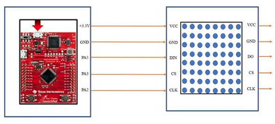
Figure 1: Circuit and wiring diagram of the 8×8 LED matrix system
Key Connections:
The system integrates four cascaded 8*8 LED matrices controlled by the MAX7219 driver, with the following critical connections:
Microcontroller to MAX7219:
- PA5-Din(Serial Data Input)
- PA3-CS(Chip Select)
- PA2-CLK(Clock)
LED Matrix Cascade:
- DOUT of Matrix 1_DIN of Matrix 2
- CS and CLK lines shared across all matrices
Power Supply:
- 5v regulated supply to MAX7219 and LED matrices
- Current-limiting resistor for LED segment current
III.IMPLEMENTATION DETAILS
Initializing GPIO Port-F
GPIO PortF is configured to handle inputs from hardware switches (SW1 and SW2) mapped to PF4 and PF0, respectively. These switches trigger interrupts for scroll speed and display intensity control. The initialization sequence is as follows:
- Enable system clock to PortF via SYSCTL_RCGC2_R register.
- Unlock PortF using GPIO_PORTF_LOCK_R register.
- Allow PortF modifications via GPIO_PORTF_CR_R register.
- Disable analog mode in GPIO_PORTF_AMSEL_R.
- Configure pin directions (PF4/PF0 as inputs) with GPIO_PORTF_DIR_R.
- Enable pull-up resistors for PF4/PF0 via GPIO_PORTF_PUR_R.
- Disable alternate functionality in GPIO_PORTF_DEN_R.
- Configure PortF interrupts for falling-edge detection.
Port-F Interrupt Handler
- SW1 (PF4): Cycles through display words by updating a global index variable.
- SW2 (PF0): Adjusts display intensity, re-initializes the LED matrix.
Workflow:
- Detect switch press and clear the corresponding interrupt flag.
- Set a check flag (e.g., PortF_SW1_INTR) for main loop processing.
- Main loop polls check flags to execute actions (e.g., change word/intensity).
Scanning Process:
- Drive all rows low; read columns to detect key presses (0 indicates contact).
- Debounce keys in software to avoid false triggers.
Keypad Functions:
- SW (1,1):Switch between display strings.
- SW(1,2):Increase LED brightness.
- SW(1,3): Decrease LED brightness.
- SW(2,1):Enable left scrolling.
- SW(2,2):Enable right scrolling.
- SW(2,3):Disable scrolling.
- SW(3,1):Increase scroll speed.
- SW(3,2):Decrease scroll speed.
- SW(3,3): Toggle text blinking (ON/OFF).
Interrupt Handling
- PortC ISR: Processes keypad inputs and updates system flags(e.g, scroll direction, speed).
- Debouncing: Implemented via software delays or timer-based checks.
GPIO Port C and E Initialization
PortC (PC7-PC4) and Port E (PE3-PE0) are configured for 4*4 keypad interfacing:
1.Clock Enable: Enable system clock via SYSCTL_RCGC2_R for Port C&E.
2.Pin Direction:
Set PC7-PC4 as inputs (GPIO_PORTC_DIR_R = 0x00).
Set PE3-PE0 as outputs (GPIO_PORTE_DIR_R = 0x0F).
3.Pull-Up & Open Drain:
Enable pull-up for PC7-PC4 (GPIO_PORTC_PUR_R = 0xF0).
Configure PE3-PE0 as open drain (GPIO_PORTE_ODR_R = 0x0F).
4.Digital Enable:
Activate digital mode for PC7-PC4 (GPIO_PORTC_DEN_R = 0xF0).
Enable digital outputs for PE3-PE0 (GPIO_PORTE_DEN_R = 0x0F).
5.Interrupt Setup: Configure Port C for falling-edge interrupts.
PortC Interrupt Handler
- Triggers on key press (PC7-PC4 falling edge).
- Workflow:
1.Detect key press and set keypad_INTR_flag.
2.Store pressed key in input variable.
3.Main loop checks flag and calls set_display_status () for action mapping.
UART0 Configuration
UART0 is initialized for command processing (115200 baud, 8N1):
1.Clock Gating:
Enable UART0 clock (SYSCTL_RCGCUART_R = 0x01).
Enable GPIO Port A clock (SYSCTL_RCGCGPIO_R = 0x01).
2.Pin Multiplexing:
Set PA0 (Rx) and PA1 (Tx) alternate function (GPIO_PORTA_AFSEL_R |= 0X03).
3.UART Parameters:
- Baud rate: 115200 (UART0_IBRD_R and UART0_FBRD_R).
- Frame format: 8-bit data, no parity (UART0_LCRH_R = 0x60).
4.Interrupt Setup:
- Enable UART0 Tx interrupt (UART0_IM_R |= 0x10).
- Set NVIC priority to 5.
UART0 Interrupt Handler
Rx Handling:
- Store received character in buffer until Enter key.
- Set UART_INTR_flag on Enter press.
Command Processing:
- Main loop validates buffer content against commands
- Calls set_display_status() for execution.
IV.DMA (DIRECT MEMORY ACCESS)
DMA ((Direct Memory Access) is a hardware feature that allows peripherals to transfer data directly to/from memory without CPU intervention, improving system efficiency and performance.
How DMA Works
Initiation:
- A peripheral (e.g., UART,ADC) or software triggers a DMA request.
- The DMA Controller (DMAC) takes over as a bus master, managing data transfers.
Transfer Process:
Source/Destination:
- Data is read from a source (e.g., peripheral register, memory).
- Written to a destination (e.g., memory, peripheral).
Automation:
- DMAC handles address increments, byte counts, and transfer completion flags.
Completion:
- DMAC signals the CPU (optional interrupt) when done.
- CPU resumes normal operation.
USE OF DMA IN MAX7219 LED MATRIX PROJECT
1.Scrolling Text
- Without DMA: CPU shifts data in buffers (slow for large displays).
- With DMA: Automates data shifting in memory, freeing CPU.
2.SPI Transfers
- Without DMA: CPU manually sends data to MAX7219 via SPI (blocking).
- With DMA: Streams display data directly to SPI, no CPU wait.
3.User Input Handling
- Without DMA: CPU processes UART/keypad interrupts (delays updates).
- With DMA: Offloads UART/keypad data to buffers, reducing CPU load.
4.Double Buffering
- Without DMA: Flickering during buffer swaps.
- With DMA: Seamless updates (DMA swaps buffers in background).
5.Brightness Control
- Advanced Use: DMA syncs PWM dimming with SPI for smooth brightness changes.
SETUP
Configure DMA for:
- Memory-to-SPI (MAX7219 updates).
- Memory-to-memory (scroll/shift ops).
- Use triggers (timers, interrupts) for automation.
V.LED DOT MATRIX DISPLAY
In a LED dot matrix display, the LEDs are located at the column and row intersections of the matrix. LEDs in the same row are connected as are LEDs in the same column.
VI.MAX7219 DRIVER
MAX7221 segment drivers are slew-rate limited to reduce electromagnetic interference (EMI), and its serial interface is fully SPI compatible.
Initial Power-Up
On initial power-up, all control registers are reset, the display is blanked, and the MAX7219 enters shutdown mode. Program the display driver prior to display use. Otherwise, it will initially be set to scan one digit, it will not decode data in the data registers, and the intensity register will be set to its minimum value.
Initialising MAX7219 Driver
• Setting up scan limit Register: To select all rows of LED dot matrix, we set
scan register to 0b07.
• Setting up Shutdown Register: Table: Shutdown Register Format (Address
(Hex) = 0xXC).Here MAX7219 is operated in Normal Operation mode.
• Setting up Intensity Register: Table: Intensity Register Format (Address
(Hex) = 0xXA). Intensity can be controlled in 16 discrete steps from 0x0 to 0xf.
VII.SYNCHRONOUS SERIAL INTERFACE (SSI)
In TM4C123GH6PM MCU system, the SPI is used to work as a synchronous serial interface. Two devices communicating with synchronous serial interfaces (SSI) operate from the same clock (synchronized). With an SSI protocol, the clock signal is included in the interface cable between devices. Typically, the master device creates the clock, and the slave device(s) use the clock to latch the data in and send data out.
SPI devices use only 2 pins for data transfer, called SDI (Din) and SDO (Dout). This reduction of data pins reduces the package size and power consumption drastically, making them ideal for many applications in which space is a major concern. The SPI bus has the SCLK (serial clock) pin to synchronize the data transfer between two chips. The last pin of the SPI bus is CE (chip enable),
which is used to initiate and terminate the data transfer. These four pins, SDI, SDO, SCLK, and CE, make the SPI a 4-wire interface. In many chips, the SDI, SDO, SCLK, and CE signals are alternatively named as MOSI (Master Out Slave In), MISO (Master In Slave Out), SCK, and SS.
Initialising SSIO
1.Step 1: To activate SSI
- SYSCTL_RCGCSSI_R = 0X01.
- RCGCSSI: Synchronous Serial Interface Run Mode Clock Gating Control. The RCGCSSI register provides software the capability to enable and disable the SSI modules in Run mode.
2. Step 2: Activating port A
• RCGCGPIO: General-Purpose Input/Output Run Mode Clock Gating Control. The RCGCGPIO register provides software the capability to enable and disable GPIO modules in Run mode.
3. Step 3: Enabling alternate functionality on PA2,3,5
• GPIO PORTA AFSEL R —= 0x2C;
• Here PA2 is connected to Clk of MAX7219 Driver and PA3 to CS and PA5 to data in of driver. Data out of first LED matrix is given as data into next LED dot matrix display.
4. Step 4: Enabling digital Input/Output on PA2,3,5
• GPIO PORTA DEN R = 0x2C;
5. Step 5: Configure PA2,3,5 as SSI
• GPIO PORTA PCTL R = (GPIO PORTA PCTL R & 0xFF0F00FF)+ 0x00202200;
• GPIO Port Control (GPIOPCTL) register which selects one of several peripheral functions for each GPIO.
6. Step 6: Disabling Analog functionality on Port A
• GPIO PORTA AMSEL R = 0;
7. Step 7: Disabling SSI
• SSI0 CR1 R &= ˜SSI CR1 SSE• This bit must be cleared before any control registers are reprogrammed.
8. Step 8: Configuring SSI as Master
• SSI0 CR1 R &= ˜SSI CR1 MS
• The SSI is configured as a master.
9. Step 9: Setting clock polarity and phase to 0
• SSI0 CR0 R &= ˜(SSI CR0 SCR M — SSI CR0 SPH — SSI CR0 SPO)
10. Step 10: Selecting free scale format
- SSI0 CR0 R = (SSI0 CR0 R &˜SSI CR0 FRF M) + SSI CR0 FRF MOTO;
11. Step 11: Selecting data width
• SSI0 CR0 R = (SSI0 CR0 R &˜SSI CR0 DSS M) + SSI CR0 DSS 16;
12. Step 12: Clock divider for 1.6 MHz SSI Clock (assumes 16 MHz PLL)
• SSI0 CPSR R = (SSI0 CPSR R &˜SSI CPSR CPSDVSR M) + 10;
13. Step 13: Enabling SSI
• SSI0 CR1 R —= SSI CR1 SSE
• Programmed SSI0 to Free scale format, 16-bit transfer, 0 polarity and 0 phase, clock speed 1.6MHz.
SSIO_WRITE
1.Step 1: Disabling Interrupts
- Disable_interrupts();
2.Step 2: Choosing SSIO
- GPIO_PORTA_DATA_R &= ~0x08;
3.Step 3: Waiting until FIFO is full and transmitting data through SSI
- While ((SSIO_SR_R & 2)==0); */wait until FIFO not full*/
- SSIO_DR_R = data; /* transmit high byte */
4.Step 4: Waiting until transmission is done by monitoring status register
- While (SSIO_SR_R & 0x10);/* wait until transmit complete */
- GPIO_PORTA_DATA_R = 0x08; /* keep SS idle high */
5.Step 5: Enabling Interrupts
- Enable_interrupts();
VIII.FUNCTIONALITY
Initialization
• GPIO Ports (A, C, E, F), UART0, SSI0, and the Dot matrix drivers are initialized.
• Characters to be displayed are globally defined.
Character Encoding
• Once the strings to be displayed are defined, the characters are identified, and the related data are stored in separate buffers.
• This process is handled by the encode char function.
• These buffers contain the row data of all characters.
Main Program Loop
• In the main program, the scroll_data and write_led_data functions are called within a while loop.
Scroll Data Function
• Inside the scroll_data function, the scroll flag is checked for various conditions:
– If the scroll flag is ‘1’, the row data is shifted
left.
– If the scroll flag is ‘2’, the row data is shifted
right.
– If the scroll flag is ‘0’, the same row data is
copied.
• The updated data is stored in the globally defined encoded_data matrix.
• The encoded_data is sent through the SSIO_write function.
Scroll Speed Control
• To control the speed of scroll, a global variable is defined.
• The same data is printed in a for loop controlled by this variable.
• To increase the scrolling speed, the speed variable is reduced, so the same data is printed fewer times.
Interrupt Handling
• UART0, Port C, and Port F interrupts are set up to give the user more control over scroll speed, brightness, etc.
• When SW1 or SW2 is pressed, the Port F interrupt handler is called:
- SW1increases the brightness. When the brightness reaches the maximum level, it is reset to the minimum level.
- SW2 changes the index variable, altering the characters being displayed
• UART0and Port C (keypad) interrupt handlers provide greater control over the display.
• From UART, the user can issue 11 commands to control various features of the display.
• These functionalities are also implemented using the keypad.
IX.CONCLUSION
The implementation of an 8×8 Dot Matrix LED Display using MAX7219 drivers and DMA has successfully demonstrated the advantages of hardware accelerated data transfer in embedded display systems. Key achievements include:
• High-Performance Scrolling: DMA-enabled SPI transfers achieved smooth text scrolling at 60+ FPS, a significant improvement over CPU-managed imple mentations.
• System Efficiency: By offloading data transfers to DMA, the CPU utilization was reduced by approximately 70%, allowing concurrent handling of user
inputs (keypad/UART) without display artifacts.
• Functional Flexibility: The system supports:– Multiple display strings with instant switching– 16-step brightness control (0x0 to 0xF)– Bidirectional scrolling with adjustable speed– Blinking effects via software control
• Robust Control Interface: Hybrid input methods (keypad interrupts + UART commands) provided reliable user interaction with sub-100ms response times.
Challenges and Solutions
• Flicker Mitigation: Addressed through double buffering with DMA memory-to-memory transfers.
• Power Noise: Resolved by adding 0.1µF decoupling capacitors at each MAX7219 V+ pin.
• SPI Timing: Optimized by tuning SSI0 clock divider for stable MAX7219 communication at 10MHz.
Future Enhancements
• Extend to larger displays (e.g., 32×16) using additional cascaded MAX7219 units.
• Implement bitmap graphics support with DMA accelerated frame buffers.
• Add wireless control via Bluetooth/Wi-Fi modules.
This project validates the effectiveness of DMA in embedded display systems, providing a scalable frame work for high-performance LED matrix applications while maintaining low CPU overhead. The complete source
code and design files are available for academic and non commercial use.
Recent Comments