
EK-TM4C123GXL Launchpad UART Programming
Many of the TI ARM chips come with up to eight on-chip UART ports. They are designated as UART0 – UART7. In the EK-TM4C123GXL LaunchPad board, the UART0 port is connected to the ICDI (In-Circuit Debug Interface), which is connected to a USB connector. This ICDI USB connection contains three distinct functions:
- Programming (downloading) using LM Flash Programming software
- Debugging using JTAG (Stellaris In-Circuit Debug Interface)
- To use as a virtual COM port
Virtual COM Port
- When the USB cable connects the EK-TM4C123GXL LaunchPad board, the device driver at the host PC establishes a virtual connection between the PC and the UART0 of the TM4C123GH6PM micro controller.
- On the EK-TM4C123GXL LaunchPad, the connection appears as UART0 (PA0-PA1).
- On the host PC, it appears as a COM (/dev/ttyACM0) port and will work with communication software on the PC such as a terminal emulator (gtkterm, PuTTY, minicom, etc).
- It is called a virtual connection because there is no need for an additional cable to make this connection.
UART Base Addresses
TI TM4C123GH6PM micro controller can have up to 8 UART ports. They are designated as UART0 to UART7. The following shows their Base addresses in the memory map
- UART0 base: 0x4000.C000
- UART1 base: 0x4000.D000
- UART2 base: 0x4000.E000
- UART3 base: 0x4000.F000
- UART4 base: 0x4001.0000
- UART5 base: 0x4001.1000
- UART6 base: 0x4001.2000
- UART7 base: 0x4001.3000
UART Register Map
| Name | Offset | Tivaware Name | Description |
|---|---|---|---|
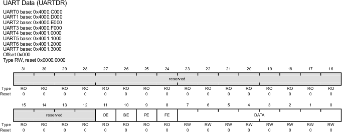
| UARTDIR | 0x000 | UARTn_DR_R | UART Data |
| UARTRSR USRTECR |
0x004 | UARTn_RSR_R UARTn_ECR_R |
UART Receive Status UARTError Clear |
| UARTFR | 0x018 | UARTn_FR_R | UART Flag |
| UARTILPR | 0x020 | UARTn_ILPR_R | UART IrDA Low-Power Register |
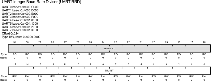
| UARTIBRD | 0x024 | UARTn_IBRD_R | UART Integer Baud-Rate Divisor |
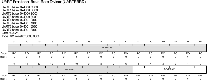
| UARTFBRD | 0x028 | UARTn_FBRD_R | UART Fractional Baud-Rate Divisor |
| UARTLCRH | 0x02C | UARTn_LCRH_R | UART Line Control |
| UARTCTL | 0x030 | UARTn_CTL_R | UART Control |
| UARTIFLS | 0x034 | UARTn_IFLS_R | UART Interrupt FIFO Level Select |
| UARTIM | 0x038 | UARTn_IM_R | UART Interrupt Mask |
| UARTRIS | 0x03C | UARTn_RIS_R | UART Raw Interrupt Status |
| UARTMIS | 0x040 | UARTn_MIS_R | UART Masked Interrupt Status |
| UARTICR | 0x044 | UARTn_ICR_R | UART Interrupt Clear |
| UARTDMACTL | 0x048 | UARTn_DMACTL_R | UART DMA Control |
| UART9BITADDR | 0x0A4 | UARTn_9BITADDR_R | UART 9-Bit Self Address |
| UART9BITAMASK | 0x0A8 | UARTn_9BITAMASK_R | UART DMA Control |
| UARTPP | 0xFC0 | UARTn_PP_R | UART Peripheral Properties |
| UARTCC | 0xFC8 | UARTn_CC_R | UART Clock Configuration |
| where n = 0 to 7 |
UART Registers Setup
There are many special function registers associated with each of the above UARTs. We will be using the UART0 as an example since a virtual connection is available on the TI Tiva LaunchPad.
Baudrate Generator (UARTIBRD)
Two registers are used to set the baud rate:
- They are UART Integer Baud-Rate Divisor (UARTIBRD) and UART Fractional Baud-Rate Divisor (UARTFBRD).
- Of the 32-bit of the UARTIBRD, only lower 16 bits are used and of the 32-bit of the UARTFBRD, only the lower 6 bits are used.
- That gives us total of 22 bits (16 bits integer + 6 bits of fraction).
- To reduce the rate of error and use the standard baud rate, we should use both of the above divisor registers when we program the baud rate.
Baudrate Generator (UARTFBRD)
Baudrate Calculation
The baud rate can be calculated using the following formula:
Desired Baud Rate = SysClk/(16 — ClkDiv)
where the SysCLK is the working system clock connected to the UART and ClkDiv is the values we load into divisor registers. The system clock fed to the CPU can come from XTAL, PLL, or an internal RC. For TI Tiva LaunchPad, the default system clock is 16 MHz. So we can rearrange the above formula as:
Desired Baud Rate = 16MHz/(16 - ClkDiv) = 1MHz/ClkDiv
The ClkDiv value gives us both the integer and fractional values needed for the UARTIBRD and UARTFBRD registers. While the integer portion of the divisor is easy to calculate using a simple calculator, the calculation of the fraction part requires some mathematical manipulation. One way would be, to multiply the fraction by 64 and round it by adding 0.5 to it.
Baudrate Calculation Example
Assume SysCLK Frequency = 16MHz. Find the values for the divisor registers of UARTIBRD and UARTFBRD for the following standard baud rates:
(a) 4800 (b) 9600 (c) 57,600 (d) 115,200
By default, 16 MHz System Clock is divided by 16 before it is fed to the UART.
Therefore, we have 16MHz/16 = 1MHz and ClkDiv = 1MHz.
(a) 1MHz/4800 = 208.3333, UARTIBRD = 208 and UARTFBRD = (0.3333 * 64) + 0.5 = 21.8312 = 21
(b) 1MHz/9600 = 104.166666, UARTIBRD = 104 and UARTFBRD = (0.16666 * 64) + 0.5 = 11
(c) 1MHz/57600 = 17.361, UARTIBRD = 17 and UARTFBRD = (0.361* 64) + 0.5 = 23
(d) 1MHz/115200 = 8.680,UARTIBRD = 8 and UARTFBRD = (0.680 * 64) + 0.5 = 44
In the above Example, it must be noted that default clock is divide-by-16. We can change it to divide-by-8 by setting to 1 the HSE bit of the UART Control (UARTCTL) register.
UART Control (UARTCTL)
The next important register in UART is the control register. It is a 32-bit register and many of the bits are unused. For us the most important bits are RXE, TXE, HSE, and UARTEN.
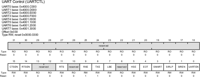
UARTEN (D0) UART enable
- This allows one to enable or disable the UART. During the initialization we must disable it while modifying some of the UART registers.
- HSE (D5) High Speed enable
- For the baud rate divisor, by default the system clock is divided by 16 before it is fed to the UART. We can change it to divide-by-8 by setting the HSE = 1 to run higher Baud rate with a low system clock frequency.
- RXE (D8) Receive enable
- We must enable this bit to receive data.
- TXE (D9) Transmit Enable
- We must enable this bit to transmit data.
- The other bits of this register are used for MODEM signals such as CTS (clear to send), RTS (request to send), parity bit, and so on.
UART Line Control (UARTLCRH)

This is the register we use to set the number of bits per character (data length) in a frame and number of stop bits among other things.
- STP2 (D3) stop bit2:
- The stop bit can be 1 or 2. The default is 1 stop bit at the end of each frame. If the receiving device is slow, we can use 2 stop bits by making the STP2 = 1.
- WLEN (D6 -D5) Word Length
- The number of bits per character data in each frame can be 5, 6, 7, or 8. Generally, we use 8 bits for each character data frame. Notice that default is 5 bits and we must change it to 8 bits as shown below:
| D6 | D5 | |
|---|---|---|
| 0 | 0 | 5 bits |
| 0 | 1 | 6 bits |
| 1 | 0 | 7 bits |
| 1 | 1 | 8 bits |
- FEN (D4) FIFO enable
- TI Tiva UART has an internal 16-byte FIFO (first in first out) buffer to store data for transmission. There is also another 16-byte FIFO buffer to save all the received bytes. By enabling FEN bit, we can write up to 16 bytes of data block into its transmission FIFO buffer and let it transfer one byte at a time.
- The programmer may set up a threshold for the UART to notify the CPU when the level of the FIFO passes the threshold.
- There is also a 16 byte FIFO for the receiver to buffer the incoming data.
- Upon Reset, the default for FIFO buffer size is 1 byte (character mode).
UART Data (UARTDR)
UART Flag Register (UARTFR)
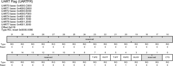
TXFE (D7) TX FIFO empty
- When we write a byte to Data register to be transmitted, the byte is placed in transmission FIFO buffer. When the transmitter is not busy, it loads one byte from the FIFO buffer and the FIFO becomes empty and the TXFE is raised. The transmitter then frames the byte and sends it out via TxD pin bit-by-bit serially.
- RXFF (D6) RX FIFO full
- When a byte of data is received, this byte is placed in Data register and RXFF (RX FIFO full) flag bit is raised. In other words, when RXFF is HIGH, it means a byte has been received.
- TXFF (D5) TX FIFOI full
- When we write a byte to Data register to be transmitted, the byte is placed in transmission FIFO buffer. When the transmitter is not busy, it loads one byte from the FIFO buffer and the FIFO is not full anymore and the TXFF is lowered. The transmitter then frames the byte and sends it out via TxD pin bit by bit serially. This is essentially the opposite of TXFE flag bit when FIFO buffer is disabled. We can monitor TXFF flag and upon going LOW we can write another byte to the Data register while the last byte is being transmitted.
- RXFE (D4) RX FIFO empty
- The received byte of data comes in serially into a Receive buffer (first bit coming in is the start bit, 8-bit data, and stop bit). After the last bit (stop bit) has been received by the receiver, the UART circuitry discards the start and stop bits and delivers a byte of data to the Data register and lowers the RXFE bit (RX FIFO empty). This is essentially the opposite of RXFF flag bit. We can monitor RXFE flag and upon going LOW (buffer not empty) we should read (retrieve) the data from Data register.
- Busy (D3)
- When a byte is written to the Data register the Busy flag goes High. While UART busy transmitting data this bit remains high until the stop bit is gone. Upon transmission of the last bit (stop bit), it goes low indicating the transmission is completed. This is only used when it is essential to complete the transmission before starting the next task.
Enabling Clock to UART (RCGCUART)
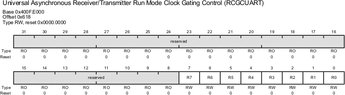
The RCGCUART register is used to enable the clock to the UART. In this register, there is a bit for each of the UART0 to UART7 modules. If a given UART is not used, we should disable the clock to it to save power. To use UART0, we set to high the D0 of this register.
The GPIO pins used for UART (TxD & RxD)
In addition to the UART registers setup, we must also configure the I/O pins used for UART for their alternate functions. In the case of UART, we need to set up GPIO pins for the alternate functions of TxD and RxD signals. In the previous examples, we used GPIO as simple I/O. We showed the minimum configuration for each port as Digital I/O and providing the Clock to it. When GPIO pins are used for their alternate peripheral functions such as UART, Timer, and ADC, we need to configure five more registers. They are PORTx Run Mode Clock Gating Control, PORTx Digital Enable, PORTx ADC Mode Selection, PORTx Alternate Selection and PORTx Port Control registers.
GPIOAMSEL (GPIO Analog Mode Select)
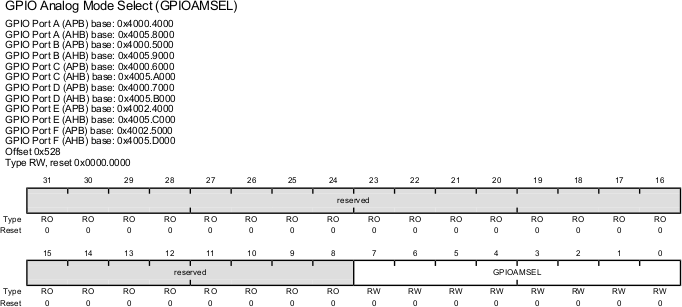
The TI ARM comes with on-chip ADC (analog to digital converter). Assume a given pins can be used for both ADC and UART and we want to use it for UART. In this case, we must isolate the ADC function since it is not used for analog operation. This is done with GPIOAMSEL (GPIO Analog Mode Selection). Although each port has its own PORTxAMSEL register, not all the pins of each port has ADC capability. Upon Reset, the PORTxAMSEL register has all 0s which means ADC function for the pin, if there is one, is disabled.
GPIO Alternate Function Select (GPIOAFSEL)

In addition to Digital I/O and Clock enable, we must also configure the alternate function select register. Upon Reset, the GPIO pins are configured for simple I/O. To use the alternate function (e.g. UART) of given pin of a given Port, there are two steps to be taken. First we must set the corresponding bits in the alternate function select HIGH. In the case of UART0, PA0 and PA1 pins are used for RxD and TxD signals, respectively. Therefore, we must set both of them high in order to be used for the alternate functions of RxD and TxD. A one in the alternate function select register tells the port pin to perform a function other than simple I/O. GPIO Alternate Function Select Register (GPIOAFSEL) needs to work with the GPIO Port Control Register (GPIOPCTL) together to determine the operational mode and related peripheral functions for the selected GPIO pins.
GPIOPCTL Register
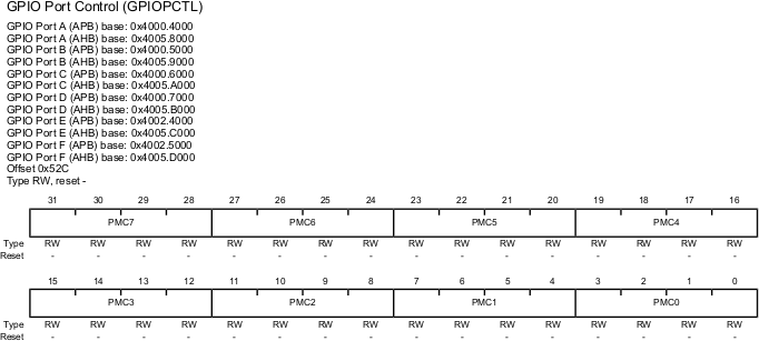
The alternate function is selected by the Port Control Register. Each 32-bit GPIOPCTL register defines the alternate function for the eight pins of that port, 4 bits for each pin. If we wished to specify PA5-2 as SSI0, we would set Port A PCTL bits 23-16 to 0x2222 like this:
GPIO_PORTA_PCTL_R = (GPIO_PORTA_PCTL_R & 0xFF0000FF) + 0x00222200;
For most of the pins, UART function select number is 1. The only exceptions are PC4 and PC5. PC4 and PC5 may be used for either UART4 or UART1. When they are used for UART4, the select number is 1. When they are used for UART1, the select number is 2.
More information on GPIO Alternate functions is available here.
Recent Comments