
II Project Overview:
With the growing demand for high-performance multimedia capabilities in embedded systems, real-time video streaming poses significant technical challenges, particularly in managing high-throughput data transfer with minimal CPU load. This mini-project focuses on designing a video streaming system using DMA on the STM32F407G- Discovery platform. The objective is to read pre-processed video data from an SD card and stream it to a 320×240 QVGA display using SPI, all orchestrated via DMA to ensure efficiency.The STM32 microcontroller was chosen for its dual independent DMA controllers,
high-frequency AHB and APB buses, and superior throughput compared to platforms like the Tiva TM4C123x. The system leverages the SDIO interface for reading video data and SPI for display communication, both enhanced with DMA transfers to avoid CPU bottlenecks. This document explores the system architecture, DMA configura-tions, data handling algorithms, and the challenges encountered during implementa-tion.
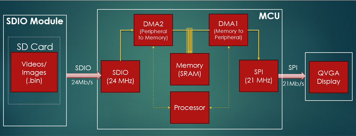
Figure 1: System Block Diagram
III Parts of the Project
3.1 STM32F407G-DISCOVERY Board Overview:
The STM32F407G-DISCOVERY board is a powerful development platform based on the ARM Cortex-M4 microcontroller, designed by STMicroelectronics. It is engi-neered for high-performance embedded applications involving real-time control, signal processing, multimedia, and communication protocols.
3.2 Microcontroller Overview: STM32F407VG:
At the core of the Discovery board lies the STM32F407VG microcontroller, which belongs to the STM32F4 series. It is built on the ARM Cortex-M4 architecture with a Floating Point Unit (FPU), offering both high computation power and low energy consumption.
• Core: ARM Cortex-M4 with FPU
• Operating Frequency: Up to 168 MHz
• Flash Memory: 1 MB
• SRAM: 192 KB (112 KB in SRAM1 + 16 KB in SRAM2 + 64 KB CCM)
• DMA Channels: 16-stream DMA controller with burst transfer capability
• Timers: 17 timers including general-purpose, PWM, and high-resolution
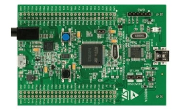
Figure 2: STM32
3.3 Key Peripherals Relevant to the Project:
• SPI: Several SPI interfaces available. SPI1 is used for high-speed data transfer to the QVGA display, configured at 21 MHz.
• SDIO: The board includes an SDIO peripheral, allowing direct interfacing with SD cards. In this project, the 1-bit SDIO mode is used at 24 MHz.
• DMA: DMA is used to efficiently move large blocks of data from SD card to SRAM without CPU intervention.
• SRAM: Dual SRAM blocks (SRAM1 and SRAM2) are used in a ping-pong con-figuration to enable continuous reading and writing in parallel.
• NVIC: Nested Vectored Interrupt Controller allows low-latency interrupt han-dling, crucial for ISR-based DMA completion triggers.
3.4 Why STM32F407 Was Chosen:
The STM32F407 is ideally suited for this application due to:
• High Clock Speed (168 MHz): Allows handling high-speed SPI and SDIO transfers.
• Efficient DMA Controller: Minimizes CPU usage and enables high-throughput data transfer.
• Dual SRAM Blocks: Facilitates parallel data handling essential for ping-pong buffering.
• Peripheral Richness: Integrates SPI, SDIO, and advanced timers needed for real-time display control.
• Free Development Tools: Supported by STM32CubeIDE and various open- source libraries.
The STM32F407G-DISCOVERY board is a powerful and versatile platform for em-bedded system development. In the context of this project, it functions as a video controller capable of real-time streaming using DMA, SPI, and SDIO. Its architecture supports efficient memory handling and high-speed communication, making it an ideal choice for implementing a smooth video streaming pipeline on a QVGA display.
IV Pin Connections:
This section describes the detailed pin configuration used in the hardware setup for interfacing the SD card (via SDIO) and the QVGA display (via SPI) with the STM32F407G-Discovery board.
4.1 SDIO Interface Connections (1-bit Mode):
The SD card is connected in 1-bit SDIO mode to the STM32 microcontroller. The specific pin assignments and power connections are as follows:
• VDD → 3.3V (power supply)
• GND → Ground
• CLK (Clock) → PC12
• D0 (Data line) → PC8
• CMD (Command line) → PD2
This configuration ensures compatibility with the STM32’s internal SDIO peripheral using 1-bit mode at 24 MHz.
4.2 SPI Interface Connections for QVGA Display:
The QVGA display communicates with the STM32 via the SPI protocol. The display
also has power and control signal lines connected as follows:
• VDD (3.3V) → 3.3V supply
• VDD (5V) → 5V supply (for backlight and power)
• GND → Ground
• Background (Backlight) → 5V
• SDI (MOSI) → PB15
• SCS (Chip Select) → PB6
• RESET → PB8
• SCL (SPI Clock) → PB13
• SDC (Data/Command Select) → PB7
This SPI connection operates at 21 MHz in SPI mode 0 (CPOL=0, CPHA=0), and only the write operation is used, making the connection unidirectional and optimal for display streaming.
4.3 Direct Memory Access (DMA):
Direct Memory Access (DMA) is a hardware feature that allows peripherals to transfer data to and from memory without continuous CPU intervention. This signif-icantly reduces processor load and increases overall system performance, especially in high-throughput applications such as video streaming.
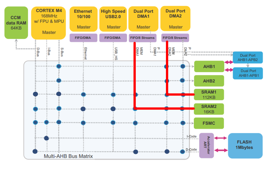
Figure 3: Multi-Bus Architecture
Working Principle of DMA
In traditional data transfer, the CPU reads data from one peripheral (e.g., SD card) and writes it to another (e.g., SRAM or display). This causes delays and consumes valuable processor cycles. DMA overcomes this by operating independently from the CPU, managing memory transactions directly using a dedicated controller.
• The CPU first configures the DMA controller by setting source and destination addresses, transfer size, and control flags.
• Once enabled, the DMA handles the data transfer in the background.
• An interrupt (DMA complete) is generated when the transfer is finished, allowing the CPU to respond or initiate the next action. DMA in This Project
In this project, DMA is used in two major roles:
1. From SD Card to SRAM: DMA reads 15 KB chunks from the SD card (via SDIO 1-bit interface at 24 MHz) and stores it into one of two SRAM blocks using a ping-pong strategy. This prevents CPU involvement during heavy data transfer and ensures seamless frame loading.
2. From SRAM to Display: After buffering, DMA is also responsible for transmit-ting the RGB565 data from SRAM to the Kentec QVGA display over SPI at 21 MHz. This allows for smooth, uninterrupted video streaming.
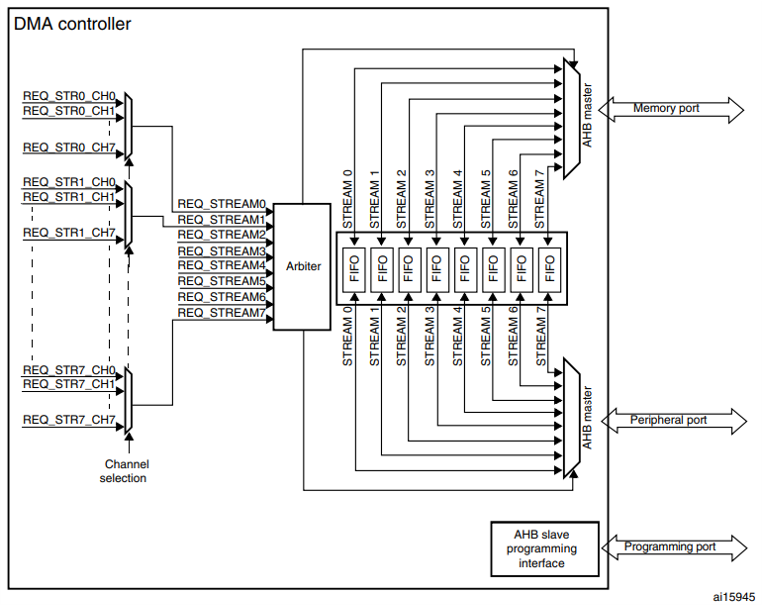
Figure 4: DMA architecture
Advantages of DMA:
• Minimized CPU Load: The CPU only initializes the DMA and handles inter-rupts, freeing it for other tasks or power-saving modes.
• Faster Transfers: DMA enables fast and deterministic data transfer, critical for real-time multimedia applications.
• Efficient Buffering: Working with double SRAM blocks and ping-pong logic, DMA ensures continuous read/write operations without collision.
DMA Controller Features in STM32F4
• 2 DMA controllers (DMA1 and DMA2)
• 16 channels (streams) and 8 requests per DMA
• Support for memory-to-memory, peripheral-to-memory, and memory-to-peripheral transfers
• FIFO support and burst transfers for enhanced speed
• Interrupt flags for half/full transfer and error handling
In summary, DMA is the backbone of this system’s real-time performance, bridg-ing peripherals and memory at high speed without CPU bottlenecks. Its integration with SDIO, SRAM, and SPI makes it an essential component of the video streaming pipeline.
4.4 Binary Conversion Process:
To enable efficient and real-time video streaming on the embedded system, it is crucial to preprocess the video data into a format that can be directly interpreted by the microcontroller and displayed on the QVGA screen. The original video file must be converted into a raw binary format with specific resolution and color depth. This section outlines the complete binary conversion workflow.
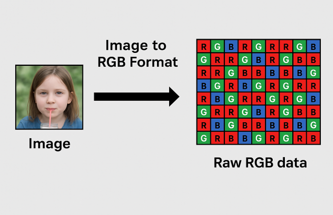
Figure 5: Conversion to Binary
4.5 Preprocessing Workflow:
The following steps were undertaken to convert a standard video into a binary file suitable for streaming:
• Frame Extraction: The input video was converted into a sequence of image frames at a rate of 15 frames per second (fps). This frame rate was selected to balance visual fluidity with the data throughput capabilities of the STM32F407 system.
• Resolution Scaling: Each extracted image was resized to a resolution of 320×240 pixels, which matches the native resolution of the Kentec QVGA display used in the project. This ensures that each pixel in the binary data maps directly to a pixel on the screen.
• Color Depth Conversion: The default color format for most images is 24-bit RGB (8 bits per channel). For embedded display applications, this is often too memory-intensive. Hence, the images were converted to 16-bit RGB565 format. In
RGB565:
– Red uses 5 bits (0–31)
– Green uses 6 bits (0–63)
– Blue uses 5 bits (0–31)
This reduces memory usage while maintaining sufficient visual quality for display purposes.
• Pixel Packing: After color depth conversion, each pixel occupies 2 bytes. The pixel data for each frame is stored in a row-major order — meaning pixels are arranged left to right, top to bottom.
• Binary Encoding: Each processed image is saved in raw binary format with a ‘.bin‘ extension. The binary data contains no headers or metadata — only the raw pixel values — to ensure compatibility with the memory-to-display DMA streaming logic.
• Binary File Merging: All individual frame binaries are then concatenated into a single large binary file. This final ‘.bin‘ file represents the complete video sequence and can be streamed frame by frame by the microcontroller.
4.6 Advantages of Binary Conversion:
This preprocessing pipeline offers several key advantages:
• Speed: Binary format removes the need for decoding or conversion on the embed-ded device, enabling direct memory access for fast rendering.
• Compactness: RGB565 format reduces the data size by one-third compared to 24-bit RGB, conserving memory and bandwidth.
• Simplicity: Using uniform binary files simplifies the embedded-side code since each frame has a fixed size and format.
10/27Embedded system design – mini project-Mtech-2025
• Deterministic Access: The system can calculate the memory offset for any frame quickly using simple arithmetic.
This binary conversion process is a critical foundation that enables the STM32 to stream video efficiently to the display using DMA and SPI, without the need for real- time image processing or format conversion.
4.7 SD Card Interface and Data Storage:
The binary video data generated through the preprocessing pipeline is stored on a microSD card, which acts as the primary external storage medium for the video frames. The STM32F407G microcontroller accesses this data using the Secure Digital Input Output (SDIO) interface.
4.8 Secure Digital (SD) Card:
An SD card is a non-volatile memory card commonly used in embedded systems for mass storage. It supports different file systems (e.g., FAT32, exFAT) and provides block-level access to data. In this project, a 64 GB microSD card is used to store the binary file containing video frames. The binary file is written to the SD card using a computer before being inserted into the embedded system.
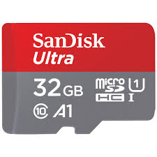
Figure 6: SD Card
Storage Format: The SD card contains a single ‘.bin‘ file representing the entire video stream.
• Block Access: Data from the binary file is read in chunks (typically 512-byte blocks) by the STM32 using DMA.
4.9 SDIO Interface Overview:
SDIO (Secure Digital Input Output) is a hardware interface used by microcontrollers to communicate with SD cards and other SDIO-compatible peripherals. Unlike SPI mode (often used in simpler MCUs), SDIO offers higher data transfer rates and greater efficiency by supporting parallel data lines and hardware-managed protocols.
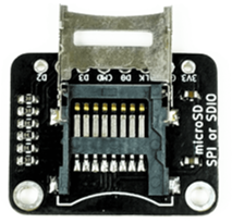
Figure 7: SDIO
4.9.1 Operating Modes of SDIO
SDIO supports multiple bus widths for communication:
• 1-bit Mode: Data is transferred over a single data line.
• 4-bit Mode: Four data lines are used in parallel, increasing throughput. 4.10
1-bit Mode Operation at 24 MHz
In this project, the SDIO peripheral of the STM32F407 is configured in 1-bit mode and operated at a clock frequency of 24 MHz. Although SDIO supports 4-bit mode for higher speeds, the 1-bit mode was selected due to its simplicity and compatibility with the available hardware and firmware configuration.
4.10.1 Why 1-bit Mode?
• Pin Limitation: 1-bit mode reduces the number of required GPIO pins, which is advantageous in resource-constrained designs.
• Stability: 1-bit mode often provides more reliable communication, especially with long wires or noisy environments.
• Ease of Configuration: The firmware configuration and driver support for 1-bit mode is simpler and more robust for beginner-level and mid-complexity applica-tions.
4.10.2 Throughput Calculation:
In 1-bit SDIO mode operating at 24 MHz:
Theoretical Data Rate = 24 Mbps = 3 MB/s
Given that each video frame is approximately 153.6 KB and the frame rate is 15 fps, the required throughput is:
15 × 153.6 KB = 2.304 MB/s
Thus, the 1-bit SDIO mode at 24 MHz provides sufficient bandwidth for continuous streaming of video frames without buffer underflows or timing violations.
4.11 DMA Integration with SDIO:
The STM32’s SDIO interface is used in conjunction with DMA2 to transfer data blocks directly from the SD card into system memory. This offloads the CPU and enables high-speed data acquisition without blocking the main application loop.
• Burst Mode: DMA is configured in burst mode with FIFO enabled to improve transfer efficiency.
• Block Size: Transfers are aligned to 512-byte sectors as per SD card protocol. 4.12
Benefits of SD Card Usage in Embedded Streaming
• Large Storage Capacity: Easily supports multi-minute or full-length videos without requiring onboard flash.
• Hot-swappability: Binary files can be replaced or updated without reprogram-ming the microcontroller.
• Modularity: The use of external storage decouples video data from firmware, simplifying project maintenance and updates.
4.13 DMA-Based Data Transfer from SD Card:
Efficient and high-speed data transfer from the SD card to memory is crucial for real- time video streaming. In this project, the Direct Memory Access (DMA) controller of the STM32F407 microcontroller is configured to work with the SDIO interface in 1-bit mode to read video data stored in FAT format. This section discusses the theory and implementation of this mechanism.
4.14 Direct Memory Access (DMA) Overview:
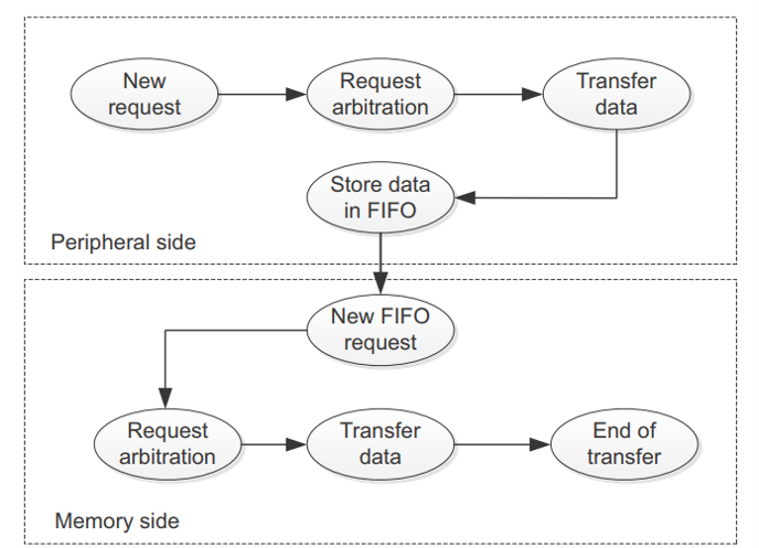
Figure 8: Peripheral To Memory DMA request
DMA is a hardware feature that allows data to be transferred directly between peripherals and memory, or between memory locations, without CPU intervention. This leads to reduced CPU load, faster data movement, and increased efficiency—especially in real-time applications such as video playback or sensor data acquisition.
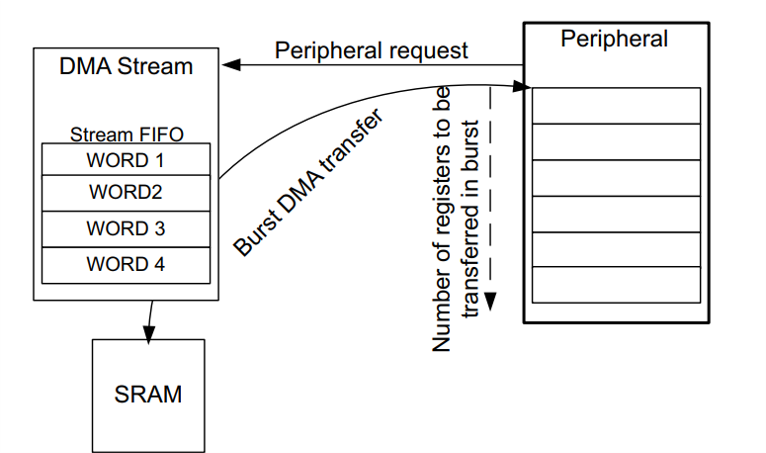
Figure 9: DMA burst mode
• Non-blocking Transfers: Once configured, the DMA handles the entire transfer independently.
• Interrupt-based Completion: Upon transfer completion, the DMA triggers an interrupt to notify the CPU.
• High Throughput: DMA operates at bus speed, enabling faster data handling than software-based methods.
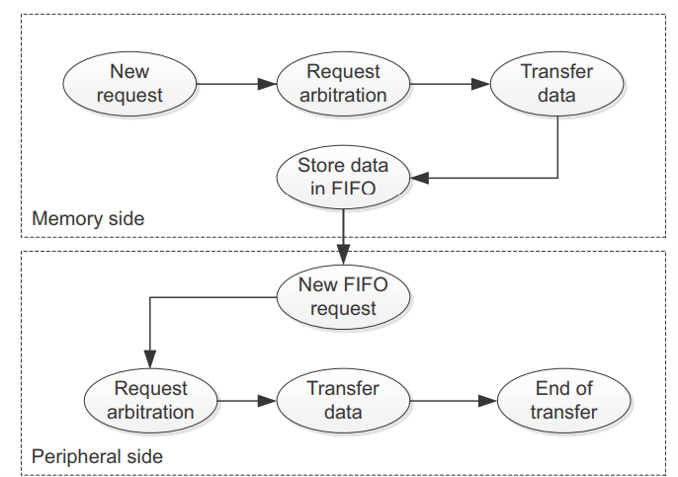
Figure 10: Memory To Peripheral DMA request
4.15 File System: FAT Mode:
The SD card is formatted using the FAT (File Allocation Table) file system. FAT32 is widely supported in embedded systems and offers:
• Compatibility with SDIO + FATFS libraries (e.g., Chan’s FatFs)
• File-based access to large binary files
• Simple API for reading specific byte offsets using functions like f read()
4.16 Reading in 15 KB Blocks:
To maintain a consistent video frame rate and manage memory usage efficiently, data is read in chunks of 15 KB (15,360 bytes). This size is carefully chosen because:
• It fits well within the STM32’s SRAM limits.
• It can store approximately 2 full frames of 320×240 pixels in RGB565 format (each frame is 153.6 KB).
• Smaller, manageable chunks reduce latency and allow time for display and prefetching.
4.17 Ping-Pong Buffering Using Dual SRAM Blocks
To ensure continuous and seamless video playback without stalling, a technique called ping-pong buffering is implemented. Two memory buffers (Buffer A and Buffer B) are defined in SRAM. The concept works as follows:
• While Buffer A is being displayed to the screen, DMA fills Buffer B with the next chunk of data from the SD card.
• Once Buffer B is filled (15 KB), an interrupt is triggered to signal the application.
• The buffers then swap roles: Buffer B is displayed while DMA refills Buffer A.
• This process repeats, providing uninterrupted data flow.
4.18 Interrupt-Driven DMA Management:
After each 15 KB block is read using DMA, a transfer complete interrupt is triggered.The interrupt service routine (ISR) handles the following:
• Updates a flag indicating that a buffer is ready to be used.
• Switches the active and inactive buffers.
• Initiates the next DMA transfer into the now-inactive buffer.
This mechanism ensures minimal CPU workload, as the CPU is only responsible for high-level buffer management and initiating the next transfer cycle. All heavy data movement occurs in the background.
4.19 Advantages of Ping-Pong DMA with SDIO:
• No Data Loss: One buffer is always being prepared while the other is in use.
• Continuous Streaming: Provides a smooth video output without delays or frame drops.
• Efficient Memory Usage: Reduces the need for a large frame buffer by overlap ping computation with data loading.
• Minimal Latency: Quick ISR response ensures uninterrupted playback.
4.20 System Flow Summary:
1. System reads 15 KB from the SD card using DMA into Buffer A.
2. Once DMA completes, it raises an interrupt.
3. ISR swaps Buffer A and B.
4. While the newly filled buffer is being displayed, another 15 KB is fetched into the other buffer.
This double-buffering DMA strategy is essential for maintaining a 15 fps frame rate without bottlenecks in a resource-constrained embedded environment.
V Ping-Pong Buffering and Dual-SRAM Optimization:
To ensure uninterrupted and real-time data streaming for video playback, a method called ping-pong buffering is employed using two separate SRAM memory blocks in the STM32F407 system. This section explains the theoretical foundation of ping-pong buffering, why dual SRAM is beneficial, and the two algorithmic approaches used in this project for memory access and display scheduling.
5.1 Theory of Ping-Pong Buffering:
Ping-pong buffering, also known as double buffering, is a technique used in systems that require simultaneous reading and writing of data. Instead of using a single buffer for both operations—which would lead to contention and delays—two buffers are used alternately.
• While Buffer A is being filled with new data (write operation), Buffer B is used to display previously loaded data (read operation).
• Once Buffer A is full, the roles are swapped—Buffer A is read, and Buffer B is written.
• This cycle continues, providing smooth data flow and eliminating wait time between operations.
5.2 Advantages of Ping-Pong Buffering:
• Prevents Data Overlap: Avoids overwriting data that is still being processed.
• Maintains Throughput: Enables continuous data movement without delay.
• Decouples Processes: Reading and writing tasks operate independently and in parallel.
• Low CPU Load: Works seamlessly with DMA and ISR to minimize CPU involvement.
5.3 Dual-SRAM Implementation for Parallel Access:
The STM32F407 microcontroller provides multiple SRAM regions (e.g., SRAM1 and SRAM2), which can be used in parallel. In this project, the two buffers for ping-pong buffering are placed in different SRAM regions:
• SRAM Block 1: Holds one of the ping-pong buffers.
• SRAM Block 2: Holds the other ping-pong buffer.
5.3.1 Why Use Two SRAM Blocks?
Using separate memory banks allows simultaneous access to both buffers—one by DMA for writing and one by the display logic for reading—without memory access conflicts.
• Parallelism: Memory controller can access both blocks simultaneously.
• No Wait States: Prevents delays caused by memory contention in single-SRAM usage.
• Higher Efficiency: Improves data throughput and frame timing precision.
5.3.2 What if Only One SRAM Block Is Used?
If both buffers were allocated in the same SRAM block:
• The DMA and display controller would compete for access to the same memory.
• This results in wait states, leading to stalling of one process while the other executes.
• Continuous video playback might suffer from flickering, tearing, or dropped frames.
5.4 Ping-Pong Algorithm Approaches
Two approaches were implemented for scheduling the read and write cycles to/from the SRAM buffers:
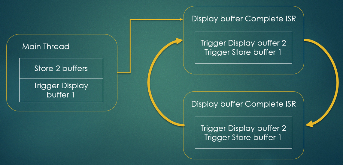
Figure 11: Algorithm 1
5.4.1 Method 1: Alternating Read/Write with Overlap:
1. Load 15 KB of data into SRAM1 using DMA from SD card.
2. Then load the next 15 KB into SRAM2.
3. Start displaying the data from SRAM1.
4. Once SRAM1 is finished displaying, switch to SRAM2.
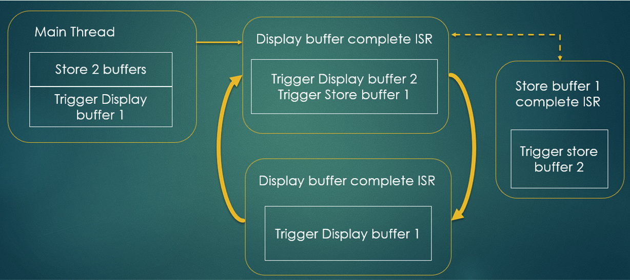
Figure 12: Algorithm 2
5. In parallel, the next set of data is loaded back into SRAM1, while SRAM2 is being displayed.
6. This alternate cycle continues in a loop.
Advantages:
• Simple to implement and manage.
• Full control over buffer switches and DMA cycles.
• Low risk of timing issues.
5.4.2 Method 2: Simultaneous Pre-Filling Both Buffers
1. Preload SRAM1 and SRAM2 in sequence before starting display.
2. Begin display from SRAM2.
3. While display continues from SRAM2, load new data into SRAM1 and SRAM2 simultaneously or back-to-back with minimal delay.
4. At the end of each frame cycle, both buffers are updated with new data, and the display continues.
Advantages:
• Better suited for high frame rate or high-resolution applications.
• Reduces idle time between transfers.
5.5 Final Remarks on Ping-Pong Strategy:
The ping-pong method, especially when enhanced using multiple SRAM blocks, ensures continuous video playback from SD card to display without CPU intervention.It provides the timing predictability and efficiency required in real-time embedded systems, particularly in video streaming applications.This optimized dual-buffer strategy is fundamental to the architecture of the system,balancing memory bandwidth and display requirements.
VI SPI-Based Display Streaming from SRAM:
After retrieving and buffering the video data from the SD card into SRAM using DMA, the next phase involves sending the image data from SRAM to the QVGA display. This is accomplished using the SPI (Serial Peripheral Interface) communication protocol configured in Mode 0 (CPOL=0, CPHA=0) and clocked at 21 MHz.The implementation uses a dual-SRAM ping-pong model to ensure continuous data
streaming.
6.1 Theory of SPI Communication:
Serial Peripheral Interface (SPI) is a synchronous serial communication protocol used for short-distance communication, typically between microcontrollers and peripherals such as displays, sensors, and memory devices.
• Full Duplex: SPI allows simultaneous transmission and reception.
• Clock Polarity and Phase: In Mode 0, CPOL = 0 (clock idle low), and CPHA= 0 (data sampled on the rising edge).
• High-Speed Capability: SPI can operate at much higher frequencies than protocols like I2C.
• Master-Slave Architecture: One master controls the bus and initiates communication with slave devices.
6.2 Theory of SRAM (Static RAM):
SRAM is a type of volatile memory that does not need to be refreshed, unlike DRAM. It provides faster access times and is ideal for storing data temporarily in real-time embedded systems.
• Low Latency: Immediate access to data.
• Random Access: Any memory location can be read or written in constant time.
• Dual-Port Possibility (if separate blocks): Two SRAM blocks can be accessed in parallel with no contention.
In STM32F407, SRAM1 and SRAM2 are independent blocks and can be accessed simultaneously.
6.3 SPI to Display: System Design:
The data buffered in SRAM (using DMA from SD card) is transmitted to the QVGA display using the SPI interface configured as follows:
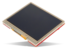
Figure 13: Kentec
• SPI Mode: Mode 0 (CPOL = 0, CPHA = 0).
• Clock Speed: 21 MHz SPI clock to support fast pixel streaming.
• Data Width: Each pixel is 16 bits (RGB565 format).
• Display Resolution: 320 × 240 (QVGA).
6.4 Memory Read Strategy: Jumping Between SRAM Blocks:
To ensure a seamless flow of pixel data to the display, a ”jumping” algorithm is implemented over the dual-SRAM buffers.
Concept: While one SRAM block is being filled with data from the SD card (via DMA), the other SRAM block is read continuously by the SPI interface for displaying.
6.4.1 Why Jump Between SRAM Blocks?
• Avoid Stalls: If only one block is used, SPI may attempt to read from a block that is being written by DMA, causing contention.
• Parallelism: Independent blocks allow simultaneous read (SPI) and write (DMA).
• Consistent Frame Rate: Enables continuous streaming at the target 15 fps without data access bottlenecks.
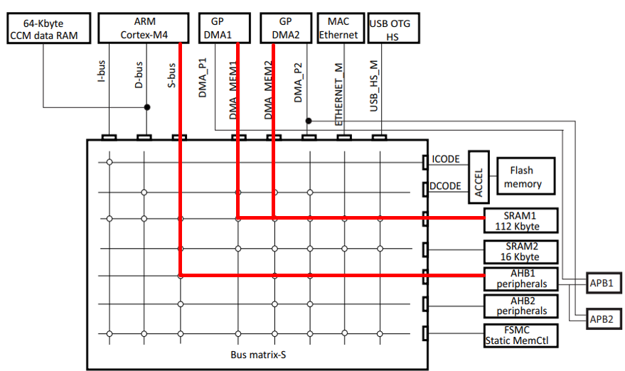
Figure 14: Bus Matrix
6.5 Algorithm for SPI Streaming:
1. The SPI master (STM32) begins reading from SRAM1, sending 16-bit pixel data to the QVGA display.
2. As soon as SRAM1 is completely read, the system jumps to SRAM2 and begins reading.
3. Meanwhile, data is again being filled into the other SRAM block from SD card via DMA.
4. This back-and-forth ”jumping” continues to maintain an uninterrupted pixel stream to the display.
6.6 Key Benefits of This Design:
• Real-Time Display: No flickering or delay due to dedicated read buffer.
• Memory Access Optimization: Reduces wait cycles and boosts SPI throughput.
• Modular Scalability: Can be extended to more buffers or higher frame rates with suitable memory upgrades.
This SPI-SRAM-display pipeline is critical for ensuring low-latency, real-time rendering of video frames. By pairing dual SRAM blocks with high-speed SPI and an efficient ”jumping” buffer algorithm, the system achieves consistent frame output even at relatively high resolutions and frame rates for embedded displays.
6.7 Kentec QVGA Display with SPI Interface:
In this project, the display module used is the Kentec QVGA TFT LCD, which is interfaced with the STM32F407G-Discovery board. The QVGA (Quarter Video Graphics Array) resolution is 320 × 240 pixels, making it well-suited for embedded systems with constrained memory and processing capabilities.
6.8 Display Specifications:
The Kentec QVGA display module comes with several features that make it ideal for real-time embedded display applications:
• Resolution: 320 (H) × 240 (V) pixels, in 16-bit RGB565 format.
• Color Depth: 65K colors (RGB565 format – 5 bits Red, 6 bits Green, 5 bits Blue).
• Controller: Integrated graphics controller with internal memory buffer.
• Interface: Only supports SPI communication protocol.
• Backlight: LED-based for better visibility.
6.9 Inbuilt Frame Buffer Advantage:
One of the major advantages of this display is its internal frame memory. This buffer can hold a full frame of 320 × 240 pixels, which means:
• Once a complete frame is written to the display, it holds the image without requiring continuous refreshing.
• The display content remains stable until a new frame is sent.
• This significantly reduces processor overhead and improves real-time performance.
• Eliminates tearing or flickering issues common in displays that require external refreshing.
This built-in frame memory allows the system to decouple display timing from frame generation, which is highly beneficial when working with slower SD card reads and
real-time SPI transfers.
6.10 Why Use SPI for Display Communication?
The Kentec QVGA display supports only the Serial Peripheral Interface (SPI) for communication. This dictates the design of the system to use SPI for transferring pixel data.
Advantages of SPI in this Context:
• Hardware Simplicity: Requires fewer pins (MOSI, SCK, CS) compared to parallel interfaces.
• High-Speed Support: In this project, SPI is configured at 21 MHz, sufficient to handle 15 fps at QVGA resolution.
• Compatibility: Well-supported by STM32F407 hardware SPI modules.
• Streaming-Friendly: Works efficiently with DMA and ping-pong SRAM buffer architecture.
• Data is streamed from the SD card into SRAM using DMA.
• The STM32 reads pixel data from SRAM in RGB565 format.
• This data is then transmitted via SPI to the Kentec QVGA display.
• Since the display has internal frame memory, only one complete frame needs to be written per cycle.
The Kentec QVGA TFT LCD is a powerful and efficient choice for embedded video display applications. Its internal frame buffer eliminates the need for constant refreshing, and its SPI-only interface integrates seamlessly with the STM32F407G-Discovery board. Together with the optimized dual-SRAM ping-pong algorithm and DMA-based SD card reading, this system architecture provides a smooth and flicker-free video play- back experience at 15 fps.
VII Challenges Faced:
Throughout the development of the video streaming system, several technical challenges were encountered, particularly in SD card interfacing and real-time data handling. Key challenges and their solutions are detailed below:
7.1 1. Inefficiency in Reading SD Card Data Over SPI:
• When using the SPI protocol for SD card access, each 512-byte block read operation required waiting for a data token 0xFE from the card.
• The appearance of this token was both arbitrary and unpredictable, forcing the processor to poll or implement timeouts.
• This polling-based mechanism led to blocking behavior, making it unsuitable for high-throughput, real-time applications like video streaming.
• To overcome this inefficiency, we transitioned to using the SDIO protocol in 1-bit mode, which supports faster, non-blocking data transfer using DMA.
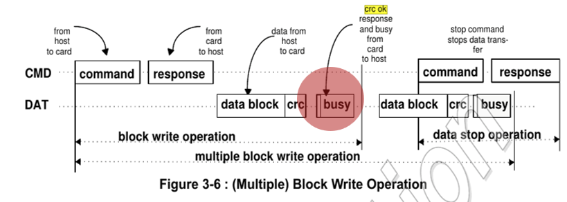
Figure 15: Reading SD card in SPI protocol
7.2 FatFs/SDIO Driver Incompatibility with Interrupt Service Routines (ISRs):
• The FatFs library and SDIO drivers internally rely on status polling and timeout- based blocking checks.
• When such functions were invoked from within an ISR context, they caused system deadlocks, as necessary resources or states were inaccessible during interrupt execution.
• To resolve this, we restructured the driver logic:
– Bypassed blocking operations within the ISR.
– Separated the actual DMA configuration and execution from the blocking FatFs wrapper functions.
• This enabled safe and non-blocking invocation of SD card reads during DMA completion interrupts.
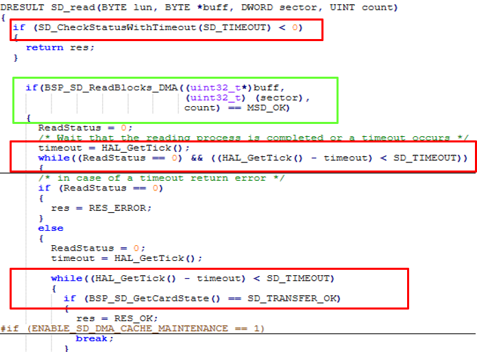
Figure 16: Modified Code
3. Custom Modifications to FatFs Functions:
• We explored the internal structure of the f read() function and broke it into smaller modular parts.
• Critical operations like buffer allocation, block address calculation, and DMA triggering were moved outside the restricted FatFs context.
• This allowed fine-grained control over memory access and real-time synchronization without depending on the internal blocking mechanisms of the library.
These modifications were essential in achieving a stable, high-performance video streaming pipeline capable of operating under the tight constraints of embedded systerms.
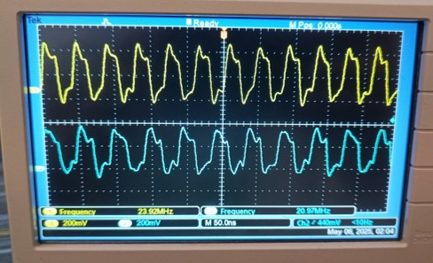
Figure 17: Oscilloscope Output
To ensure correct operation and validate timing, we measured the SDIO and SPI clock frequencies using an oscilloscope. The observed waveforms confirmed the expected 24 MHz for SDIO and 21 MHz for SPI, verifying correct peripheral configuration.
VIII Conclusion:
This mini project, titled “Video Streaming Using DMA”, demonstrates an efficient, real-time embedded video streaming pipeline built around the STM32F407G-DISCOVERY board and a Kentec QVGA display. By integrating optimized hardware interfaces and data management techniques, the system achieves stable video playback at 15 frames per second with minimal CPU overhead.
The journey began with the extraction of video frames using Python, converting them to 320×240 resolution and compressing the data from 24-bit RGB to 16-bit RGB565 format. These frames were merged into a single binary file for efficient storage and later transferred to an SD card. The SD card interface was implemented using the SDIO 1-bit mode operating at 24 MHz. This mode was chosen for its simplicity and sufficient bandwidth for continuous data streaming. To further improve efficiency, DMA was used to read data blocks of 15 KB from the SD card, triggering an interrupt upon each successful transfer.To prevent data starvation and enable continuous flow, a ping-pong buffering strategy was adopted using the dual SRAM blocks of the STM32F4. This allowed the system to simultaneously read new frame data into one SRAM block while the previous data was being displayed from the other. The ping-pong mechanism was implemented in two distinct approaches — alternating storage and parallel read-write — to ensure minimal latency and improved throughput.Following the buffering phase, data was transmitted from SRAM to the Kentec QVGA display using the SPI protocol configured in Mode 0 at 21 MHz. The display’s internal frame buffer enabled flicker-free video output without the need for constant refreshing, making it ideal for embedded video applications.At the heart of this entire system is the STM32F407G-DISCOVERY board, which, with its powerful ARM Cortex-M4 processor, integrated DMA controller, SPI, SDIO, and dual SRAM banks, enabled high-speed and deterministic video streaming. The use of interrupts and peripheral-level control allowed the CPU to operateefficiently, delegating memory transfers and peripheral access to dedicated hardware blocks.
In conclusion, this project showcases how a carefully architected embedded system can handle real-time video streaming by harmonizing frame extraction, optimized storage, intelligent memory access patterns, and display synchronization. The result is a robust and scalable framework suitable for multimedia applications, surveillance systems, or low-power video devices in the embedded domain.
Recent Comments