
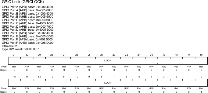
GPIO – Unlock the port
This step is only needed for pins PC0-3, PD7 and PF0 on TM4C123GXL LaunchPad.
After enabling the clock some ports are still locked. For unlocking them we would have to write this register with the magic number 0x4C4F434B.
| Bit/Field | Name | Description |
|---|---|---|
| 31:0 | LOCK | GPIO Lock A write of the value 0x4C4F434B unlocks the GPIO Commit (GPIOCR) register for write access. A write of any other value or a write to the GPIOCR register reapplies the lock, preventing any register updates. A read of this register returns the following values: 0x1: The GPIOCR register is locked and may not be modified. 0x0: The GPIOCR register is unlocked and may be modified. |
Now we have unlocked the PORT but we are not allowed to write any changes to that port. This introduces us to GPIOCR register.
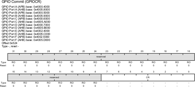
GPIO COMMIT register (GPIOCRCR)
The GPIO commit control register provides a layer of protection against accidental programming of critical hardware peripherals. Protection is provided for the GPIO pins that can be used as the four JTAG/SWD pins and the NMI pin, GPIO Pull Up Select (GPIOPUR) register, GPIO Pull-Down Select (GPIOPDR) register, and GPIO Digital Enable (GPIODEN) register are not committed to storage unless the GPIO Lock (GPIOLOCK) register has been unlocked and the appropriate bits of the GPIO Commit (GPIOCR) register have been set.
Enabling by writing 1 to the respective bit field of this register allows us to write the data to that port.
| Bit/Field | Name | Description |
|---|---|---|
| 7:0 | CR | GPIO Commit 0: The corresponding GPIOAFSEL, GPIOPUR, GPIOPDR, or GPIODEN bits cannot be written. 1: The corresponding GPIOAFSEL, GPIOPUR, GPIOPDR, or GPIODEN bits can be written. |
| 31:8 | Reserved | Software should not rely on the value of a reserved bit. |
Note:
The default register type for the GPIOCR register is RO for all GPIO pins with the exception of the NMI pin and the four JTAG/SWD pins. These six pins are the only GPIOs that are protected by the GPIOCR register. Because of this, the register type for the corresponding GPIO Ports is RW.
The default reset value for the GPIOCR register is 0x000000FF for all GPIO pins, with the exception of the NMI and JTAG/SWD pins. To ensure that the JTAG and NMI pins are not accidentally programmed as GPIO pins, these pins default to non-committable. Because of this, the default reset value of GPIOCR changes for the corresponding ports.
Recent Comments