
GPIO – Read Write Data Register (GPIODATA)
The data control registers allow software to configure the operational modes of the GPIOs. The data direction register (GPIODIR) configures the GPIO as an input or an output while the data register (GPIODATA) either captures incoming data or drives it out to the pads.
- The GPIO Data Register is located at the offset address of 0x000 from the base address of its port.
- The data register supports bit-specific addressing.
- In order to write to GPIODATA, the corresponding bits in the mask, resulting from the address bus bits [9:2], must be set. Otherwise, the bit values remain unchanged by the write.

- Similarly, the values read from this register are determined for each bit by the mask bit derived from the address used to access the data register, bits [9:2]. Bits that are set in the address mask cause the corresponding bits in GPIODATA to be read, and bits that are clear in the address mask cause the corresponding bits in GPIODATA to be read as 0, regardless of their value.
- A read from GPIODATA returns the last bit value written if the respective pins are configured as outputs, or it returns the value on the corresponding input pin when these are configured as inputs.
| If we want to access bit | Offset Constanct |
|---|---|
| 7 | 0x200 |
| 6 | 0x100 |
| 5 | 0x080 |
| 4 | 0x040 |
| 3 | 0x020 |
| 2 | 0x010 |
| 1 | 0x008 |
| 0 | 0x004 |
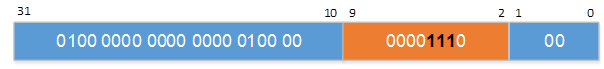
- Writing to address 0x40004038 means that bits 5, 4 and 3 of Port A must be changed.
- If we want to read and write all 8 bits of a port, it means that we need to sum all these 8 offset constants, which makes the offset address of 0x3FC (001111111100 in binary).
- If we are interested in just bit 5 of Port A, we add 0x0080 to 0x4000.4000, and we can define this in C as
#define PA5 (*((volatile uint32_t *)0x40004080))
- All bits are cleared by a reset.
Recent Comments