
DS1307 RTC Interfacing and Programming
The real-time clock (RTC) is a widely used device that provides accurate time and date information for many applications. Although some microcontrollers come with the RTC already embedded into the chip, we have to interface the vast majority of them to an external RTC chip. The DS1307 is a serial RTC with an I2C bus. In this section, we interface and program the DS1307 RTC. According to the DS1307 data sheet from Maxim, ”The clock/calendar provides seconds, minutes, hours, day, date, month, and year information”. The end of the month date is automatically adjusted for months with fewer than 31 days, including corrections for leap year. The clock operates in either the 24-hour or 12-hour format with AM/PM indicator. The DS1307 has a built-in power-sense circuit that detects power failures and automatically switches to the battery supply.” The DS1307 does not support the Daylight Savings Time option”.
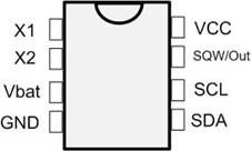
X1–X2: These are input pins that allow the DS1307 connection to an external crystal oscillator to provide the clock source to the chip. We must use a 32.768 kHz quartz crystal. The accuracy of the clock depends on the quality of this crystal oscillator.
Vbat: Pin 3 can be connected to an external +3 V lithium battery, thereby providing the power source to the chip when the external supply voltage is not available. We must connect this pin to ground if it is not used. A 48mAh lithium battery can provide the power needed for more than 10 years to power the chip.
GND: Pin 4 is the ground.
SDA: (Serial Data): Pin 5 is the SDA pin and must be connected to the SDA line of the I2C bus.
SCL: (Serial Clock): Pin 6 is the SCL pin and must be connected to the SCL line of the I2C bus.
SWQ/OUT: Pin 7 is an output pin providing 1 kHz, 4 kHz, 8 kHz, or 32 kHz frequency if enabled. This pin needs an external pull-up resistor to generate the frequency because it is open drain. If you do not want to use this pin you can omit the external pull-up resistor. We will see shortly how to control this pin.
VCC: Pin 8 is used as the primary voltage supply to the chip. This primary voltage source is generally set to +5 V. When Vcc falls below the Vbat level, the DS1307 switches to Vbat and the external lithium battery provides power to the RTC. When the system is powered on, the DS1307 automatically switches to the power supply from battery power.
Address map of the DS1307
The DS1307 has a total of 64 bytes of RAM space with addresses 00–3FH. The first seven locations, 00–06, are set aside for RTC values of time and date. The next byte is used for the control register. It is located at address 07 in hex. That leaves 56 bytes, from addresses 07H to 3FH, available for general-purpose data storage. That means the entire 64 bytes of RAM are accessible directly for read or write. The following table shows the address map of the DS1307.
| Address | Bit7 | Bit6 | Bit5 | Bit4 | Bit3 | Bit2 | Bit1 | Bit0 | Function | Range |
|---|---|---|---|---|---|---|---|---|---|---|
| 00H | CH | 10 Seconds | Seconds | Seconds | 00-59 | |||||
| 01H | 0 | 10 Minutes | Minutes | Minutes | 00-59 | |||||
| 02H | 0 | 12
24 |
10 Hour
PM/AM |
10 Hour | Hours | Hours | 1-12 +AM/PM 0-23 |
|||
| 03H | 0 | 0 | 0 | 0 | 0 | Day | Day | 01-07 | ||
| 04H | 0 | 0 | 10 Date | Date | Date | 01-31 | ||||
| 05H | 0 | 0 | 0 | 10 Month | Month | Month | 1-12 | |||
| 06H | 10 Year | Year | Year | 00-99 | ||||||
| 07H | OUT | 0 | 0 | SQWE | 0 | 0 | RS1 | RS0 | Control | – |
| 08H-3FH | RAM 56×8 | 00h-FFH | ||||||||
The DS1307 control register
As shown in the above table, the control register has an address of 07H. In the DS1307 control register, the bits control the function of the SQW/OUT pin. If the square wave output is disabled, setting the OUT bit to 1 will make the SQW/OUT pin low, and clearing the OUT bit to zero will make the SQW/OUT pin high. If SQWE (square wave enable) bit is set HIGH, the oscillator output is enabled, otherwise, it is disabled. RS1-RS0 (rate select) bits select the output frequency of the oscillator output according to the following table:
| RS1 | RS0 | Output Frequency |
|---|---|---|
| 0 | 0 | 1 Hz |
| 0 | 1 | 4.096 kHz |
| 1 | 0 | 8.192 kHz |
| 1 | 1 | 32.768 kHz |
CH bit in address 00
One of the most important bits in the Seconds (address location 00) in the DS1307 is the CH (Clock Halt) bit. It is the seventh bit of address location 00. Setting the CH bit to one disables the oscillator, while setting CH to zero enables the oscillator. The CH bit is undefined upon reset. In order to enable the oscillator, we must clear the CH during initial configuration.
Time and date address locations and modes
The byte addresses 0–6 are set aside for the time and date, as shown in the above table. The DS307 provides data in BCD format only. Notice the data range for the hour mode. We can select 12-hour or 24-hour mode with bit 6 of Hours register at location 02. When bit 6 is 1, the 12-hour mode is selected, and bit 6 = 0 provides us the 24-hour mode. In the 12-hour mode, bit 5 indicates whether it is AM or PM. If bit 5 = 0, it is AM and if bit 5 = 1 it is PM. See the following example.
What value should be placed at location 02 to set the hour to: (a) 21, (b) 11AM, (c) 12 PM
Solution:
(a) For 24-hour mode, we have D6 = 0. Therefore, we place 0010 0001 (or 0x21) at location 02, which is 21 in BCD.
(b) For 12-hour mode, we have D6 = 1. Also, we have D5 = 0 for AM. Therefore, we place 0101 0001 at location 02, which is 51 in BCD.
(c) For 12-hour mode, we have D6 = 1. Also, we have D5 = 1 for PM. Therefore, we place 0111 0010 at location 02, which is 72 in BCD.
Register pointer
In DS1307, there is a register pointer that specifies the byte that will be accessed in the next read or write command. The first read or write operation sets the value of the pointer. After each read or write operation, the content of the register pointer is automatically incremented to point to the next location. It is useful in multi-byte read or write.
Writing to DS1307
To set the value of the register pointer and write one or more bytes of data to DS1307, you can use the following steps:
- To access the DS1307 for a write operation, after sending a START condition, you should transmit the address of DS1307 (1101 000) followed by 0 to indicate a write operation.
- The first byte of data in the write operation will set the register pointer. For example, if you want to write to the control register you should send 0x07.
- Check the acknowledge bit to be sure that DS1307 responded.
- If you want to write one or more bytes of data, you should transmit them one byte at a time and check the acknowledge bit at the end of each byte sent. Remember that the register pointer is automatically incremented and you can simply transmit bytes of data to consecutive locations in a multi-byte burst write.
- Transmit a STOP bit condition.
Reading from DS1307
Notice that before reading a byte you should load the address of the byte to the register pointer by doing a write operation as mentioned before.
To read one or more bytes of data from the DS1307 we should do the following steps:
- To access the DS1307 for a read operation, you need to set the register pointer first. After sending a START condition, you should transmit the address of DS1307 (1101 000) followed by 0 to indicate a write operation (writing the register pointer).
- Check the acknowledge bit to be sure that DS1307 responded.
- The byte of data in the write operation will set the register pointer. For example, if you want to read from the control register you should send 0x07. Check the acknowledge bit to be sure that DS1307 responded.
- Now you need to change the bus direction from a transmit to receive. Send a START condition (a REPEATED START), then transmit the address of DS1307 (1101 000) followed by 1 to indicate a read operation. Check the acknowledge bit to be sure that DS1307 responded.
- You can read one or more bytes of data. Remember that the register pointer indicates which location will be read. The ACK bit in the I2CMCS register should be set for the master to acknowledge the data received. Also notice that the register pointer is automatically incremented and you can simply receive consecutive bytes of data in a multi-byte burst read.
- Before reading the last byte, clear the ACK bit in the I2CMCS register. The last byte read will have a NACK to signal the DS1307 that the burst read is complete.
- Transmit a STOP bit condition.
Recent Comments