
I2C
| OVERVIEW | I2C IN TIVA | I2C IN RTC | I2C SAMPLES | I2C TASKS |
I2C Programming in TI ARM Tiva
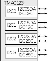
The TI ARM Tiva micro controllers have zero to ten I2C modules. The TM4C micro controllers implement just a subset of the standard. They support master and slave modes, can generate interrupts on start and stop conditions, and allow I2C networks with multiple masters. Microcontroller pins SDA and SCL can be connected directly to an I2C network, because I2C networks are intended to connect devices on the same PCB, no special hardware interface electronics are required. The I2C modules are located at the following base addresses:
| SSI Module | Base Address |
|---|---|
| I2C0 | 0x4002.0000 |
| I2C1 | 0x4002.1000 |
| I2C2 | 0x4002.2000 |
| I2C3 | 0x4002.3000 |
Table: I2C Module Base Address for TI Tiva
Enabling Clock to I2C Module
To enable and use any of the peripherals, we must enable the clock to it. We use RCGCI2C register to enable the clock to I2C modules. Notice again RCGCI2C is part of the SYSCTL registers. We need SYSCTL_RCGCI2C_R |= 0x0F, enables the clock to all four I2C modules.
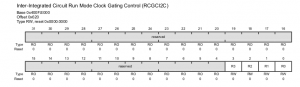
| Bits | Name | Function | Description |
|---|---|---|---|
| 0 | R0 | I2C0 Run Mode Clock Gating Control | 1: enable, 0: disable |
| 1 | R1 | I2C1 Run Mode Clock Gating Control | 1: enable, 0: disable |
| 2 | R2 | I2C2 Run Mode Clock Gating Control | 1: enable, 0: disable |
| 3 | R3 | I2C3 Run Mode Clock Gating Control | 1: enable, 0: disable |
I2C Clock speed
The I2CMTPR (I2C Master Timer Period) register allows us to set the clock rate for the SCL. The SCL clock comes from the system clock and goes through clock divider circuit controlled by I2CMTPR register. The I2C standard defines four clock speeds for the SCL. They are:
- Standard mode of 100Kbps (bits per second),
- Fast mode of 400Kbps,
- Fast Plus mode of 1Mbps. and there is also a
- High-Speed (HS) mode which can be as high as 3.3Mbps.
The lower 7 bits (D6-D0, TPR) of I2CMTPR register are used to set the I2C clock speed.
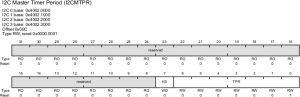
We use the following formula to set the I2C clock speed:
SCL_PERIOD = 2×(1 + TPR)×(SCL_LP + SCL_HP)×CLK_PRD
In the above formula, SCL_PERIOD is the I2C clock period, CLK_PRD is the system clock period.
- The SCL_LP is the SCL Low Period and is fixed at 6.
- The SCL_HP is the SCL High Period and is fixed at 4.
Now, if we rearrange the above formula, we have:
SCL_PERIOD = 2×(1 + TPR)×(4 + 6)×CLK_PRD
SCL_PERIOD = 2×(1 + TPR)×10×CLK_PRD
SCL_PERIOD = (20×(1 + TPR))/System_Clock_Freq
Now, solving for TPR (the value we need for the I2CMTPR register) we have:
TPR = ( (System_Clock_Freq x SCL_PERIOD) / 20 ) - 1
TPR = (System_Clock_Freq) / (20 x I2C Clock) - 1
Example: Assume the system clock frequency is 16MHz. Find the values for the I2CMTPR register if we want I2C clock of (a) 100 Kbps, (b) 400 Kbps, and (c) 1 Mbps.
Solution: Using 16MHz for the CPU Frequency, we have:
TPR = (System_Clock_Freq) / (20 x I2C Clock) – 1 ,
TPR = (16MHz) / (20 x I2C Clock) – 1
(a) TPR = (16MHz) / (20 x 100K) – 1 = 8 – 1 = 7
(b) TPR = (16MHz) / (20 x 400K) – 1 = 2 – 1 = 1
(c) TPR = (16MHz) / (20 x 1M) – 1. This is not allowed due to the system clock frequency being too low.
Master or Slave?
The I2C Module inside the ARM chip can be Master or Slave. We use I2CMCR (I2C Master Configuration register) to designate the ARM chip as master or slave. Setting bit D4 to 1 makes the I2C of ARM chip as Master. Therefore, we need
I2CMCR = 00010000 = 0x10 for Master.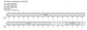
| Bits | Name | Function | Description |
|---|---|---|---|
| 0 | LPBK | I2C Loopback | 0: Normal operation, 1: Loopback |
| 4 | MFE | I2C Master Function Enable | 1: Enable Master Function, 0: Disable |
| 5 | SFE | I2C Slave Function Enable | 1: Enable Slave Function, 0: Disable |
| 6 | GFE | I2C Glitch Filter Enable | 1: Enable Glitch Filter, 0: Disable |
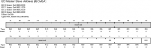
Slave Address
To transmit a byte of data to an I2C device, we must specify its I2C address. We use I2CMSA (I2C Master Slave Address) register to hold the address of the slave device. Notice, the addresses in I2C are only 7 bits (maximum of 127 devices). In the I2CMSA register, the D7-D1 bits are used for the slave address and the LSB of D0 is used to indicate if we are transmitting to slave device or receiving from a slave device.
Data Register
In Master transmit mode, we place a byte of data in I2CMDR (I2C Master Data register) for transmission. Only the lower 8 bits of this register is used.
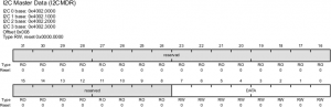
Figure: I2C Master Data (I2CMDR)
Control and Status Flag Register
We have two registers with the same name. One we write to control the I2C module, the other one we read from to get the status of the I2C module. We use the I2CMCS (I2C Master Control/Status) register for both control and status. When we write to I2CMCS register, it configures the I2C controller operation. Upon reading it, we get the status to see if a byte has been transmitted and transmission buffer is empty and ready for the next byte.
Basically we have two registers with the same name. One we write to control the I2C module, the other one we read from to get the status of the I2C module.
| Bits | Name | Function | Description |
|---|---|---|---|
| 0 | RUN | I2C Master Enable | 1: Master is enabled to transfer data |
| 1 | START | Generate START | It should be 1 to generate START condition |
| 2 | STOP | Generate STOP | It should be 1 to generate STOP condition |
| 3 | ACK | Data Acknowledge Enable | It should be 1 to generate auto ACK |
| 4 | HS | High-Speed Enable | It should be 1 to run in high speed mode |
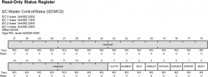
| Bits | Name | Function | Description |
|---|---|---|---|
| 0 | BUSY | I2C Busy | 0: The controller is idle 1: The controller is busy. |
| 1 | ERROR | Error | 0: No error was detected on the last operation. 1: An error occurred on the last operation. |
| 2 | ADRACK | Acknowledge Address | 0: The transmitted address was acknowledged 1: The transmitted address was not acknowledged. |
| 3 | DATACK | Acknowledge Data | 0: The transmitted data was acknowledged 1: The transmitted data was not acknowledged. |
| 4 | ARBLST | Arbitration Lost | 0: The I2C controller won arbitration 1: The I2C controller lost arbitration. |
| 5 | IDLE | I2C Idle | 0: The I2C controller is not idle. 1: The I2C controller is idle. |
| 6 | BUSBSY | Bus Busy | 0: The I2C bus is idle 1: The I2C bus is busy. |
| 7 | CLKTO | Clock Timeout Error | 0: No clock timeout error 1: The clock timeout error has occurred. |
After placing a byte of data in I2C Data register and the slave address in I2C Master Slave address register, we may write a value of 0x07 to I2CMCS register for the I2C to start a single byte data transmission from Master (microcontroller) to slave device. Notice, writing 0x07 to this register has all the three of STOP = 1, RUN = 1, and START = 1 in it. Because the START and STOP are set the I2C module will:
- generate a START condition,
- send the slave address with R/W bit,
- check the acknowledge bit,
- send the data byte,
- check the acknowledge bit and
- generate the STOP condition to terminate the transmission.
For multiple byte burst write or read, the protocols are different.
For a single byte write, after the START, the bus will go busy until the data byte is written and the STOP is sent. To monitor the progress of the transmission, we need to check the BUSBSY bit (bit 6) of the I2CMCS register. When this bit goes low, the transmission is complete.
Because ARM Cortex architecture incorporates buffered writes, the write of 0x07 to I2CMCS does not take effect immediately. Checking the BUSBSY bit immediately after setting the I2CMCS register to 0x07 may return a 0 to indicate the transmission has not started yet. To avoid this, the program should read the I2CMCS back to flush the write first before reading it again to check the BUSBSY bit.
When the transmission is complete, the program should check the ERROR bit (bit 1) to make sure there was no error in the transmission. Transmission error may be caused by either slave address was not acknowledged or the data write was not acknowledged. In either case, the ADRACK (bit 2) or the DATACK (bit 3) will be set.
In a system with multiple I2C masters, the program should check the BUSBSY (bit 6) of I2CMCS register to be sure that the bus is idle before starting a transmission. After the transmission is started, the program should check the ARBLST (bit 4) to see whether it lost the arbitration or not. If the arbitration is lost, the program should attempt the transmission after the bus is not busy anymore.
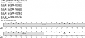
Enabling Open Drain
Most of the digital output pins are configured as totem-pole output (because the transistors of the output driver are stacked up like as totem-pole). The other name for this configuration is push-pull because it is pushing the current out when high and pulling the current in when low. This configuration allows for faster transition when the output is switching from high to low or from low to high. The problem with a totem-pole output is when more than one output is connected together and one output is high the other is low, the high outputs push the current out and the low outputs pull in the current. A large amount of current could flow between the outputs and damages the circuit.
One common solution to allow multiple outputs connected together is to use the open-drain output. (open-drain for CMOS devices or open-collector for TTL devices). In this output configuration, the output pin is connected to the drain of the output transistor while the source of that transistor is grounded. When the transistor is on, the output pin is grounded and when the transistor is off, the output pin (the drain) is open. The open-drain outputs may be connected together. A pull-up resistor is added so that the signal is high when none of the outputs is active. When any one of the outputs is active, the signal is low. It forms a “wired-AND” logic and is exactly what is required for the I2C bus.
For the I2C Module inside the TI ARM Tiva, we must enable the open-drain option for the I/O pins used by the I2C buses. We use the GPIOODR (GPIO Open Drain) register to enable the open drain. Depending on which pins we use for the I2C connection, we have to enable the GPIOODR register for that port.
Configuring GPIO for I2C
In using I2C, we must configure the GPIO pins to allow the connection of the CPU pins to I2C device pins. In this regard, it is same as all other peripherals. The steps are as follows:
- Enable the clock to GPIO pin by using RCGCGPIO.
- Set the GPIO AFSEL (GPIO alternate function) for I2C pins.
- Enable digital pins in the GPIODEN (GPIO Digital enable) register.
- Assign the I2C signals to specific pins using GPIOCTL register.
- Enable the open-drain option for the I/O pins used by the I2C signals.
- With TI Tiva devices, the I2C pins are configured as open-drain by only setting the I2CSDA pin to open-drain.
- The I2CSCL pin will become open-drain with I2CSDA.
- Setting I2CSCL pin as open-drain will not work.
| SSI Module Pin | GPIO Pin |
|---|---|
| I2C0SCL | PB2 |
| I2C0SDA | PB3 |
| I2C1SDA | PA6 |
| I2C1SDA | PA7 |
| I2C2SCL | PB4 |
| I2C2SDA | PB5 |
| I2C3SCL | PD0 |
| I2C3SDA | PD1 |
Configuring I2C for data transmission
![]()
After the GPIO configuration, we need to take the following steps to configure the I2C and send a byte of data to an I2C slave device.
- Enable the clock to I2C module using RCGCI2C (SYSCTL_RCGCI2C_R) register.
- Initialize the I2C as Master using I2CMCR (I2Cn_MCR_R) register.
- Set the I2C clock speed using I2CMTPR (I2Cn_MTPR_R) register.
- Place the slave address with the R/W bit cleared for write in the I2CMSA (I2Cn_MSA_R) register.
- Place the byte of data to be transmitted into the I2CMDR (I2Cn_MDR_R) register.
- Initiate the data transmission by writing value 0x07 to the I2CMCS (I2Cn_MCS_R) register. With I2CMCS = 0x07, will make the STOP = 1, RUN = 1, and START = 1.
- Read back I2CMCS (I2Cn_MCS_R) register to force the write out of the write buffer.
- Keep reading the I2CMCS (I2Cn_MCS_R) register and check the BUSY flag. Wait until it goes low.
- Now, read the I2CMCS (I2Cn_MCS_R) register again and check the ERROR flag to make sure there was no error.
- (Where n = 0 to 3)
To send n bytes of data, you should send the first bit like single bit transmission but leave STOP bit of I2CMCS 0 because we do not want to generate Stop Condition after sending the first byte (Instead of writing value 0x07 to the I2CMCS register, write value 0x03). Now repeat from step 5 to send more data by writing value 0x01 to the I2CMCS register. Note that you should leave the START and STOP bits of I2CMCS 0 because no Stop or Start Condition should be generated. Before sending the last byte you should make STOP bit of I2CMCS 1 to generate STOP Condition after sending the last byte of data.
Recent Comments