
LTC1661 SPI DAC
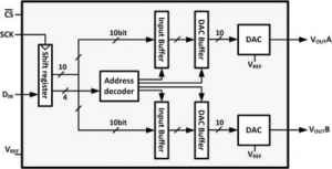
In this section we show an SPI-based DAC and its interfacing to TM4C. The LTC1661 is a 10-bit SPI serial DAC from Linear Technology. It has two separate output channels, named A and B, as shown in the following figure.
The relation between the input number and the output voltage is as follows:
VOUT = ( VREF × DIN) / 1024
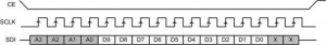
We can control the LTC1661 by sending 2 bytes of data. As shown in the following figure, the 16-bit is made of 3 parts: control code (4 bits), data (10 bits), and not used (2 bits). The control code are used to control the internal parts of the LTC1661.
As shown in above figure, each DAC is double buffered to provide simultaneous update. To do so, we load input buffers with proper values and then load the DAC buffers simultaneously. The following table shows the list of available control codes. To decrease power consumption, the DAC has a sleep mode, as well. We can switch between sleep and awake modes using proper control code.
| A3 A2 A1 A0 | Interrupt Register | DAC Register | Power Down Status |
Comments |
|---|---|---|---|---|
| 0 0 0 0 | No Change | No Update | No Change | No operation. power-down status unchanged |
| 0 0 0 1 | Load DAC A | No Update | No Change | Load input register A with data. DAC outputs unchanged. power-down Status unchanged |
| 0 0 1 0 | Load DAC B | No Update | No Change | Reserved |
| 0 0 1 1 | – | – | – | Reserved |
| 0 1 0 0 | – | – | – | Reserved |
| 0 1 0 1 | – | – | – | Reserved |
| 0 1 1 0 | – | – | – | Reserved |
| 0 1 1 1 | – | – | – | Reserved |
| 1 0 0 0 | No Change | Update Outputs | Wake | Load both DAC Regs with existing contents of input Regs. Outputs update. Part wakes up |
| 1 0 0 1 | Load DAC A | Update Outputs | Wake | Load input Reg A. Load DAC Regs with new contents of input Reg A and existing contents of Reg B. Outputs update. |
| 1 0 1 0 | Load DAC B | Update Outputs | Wake | Load input Reg B. Load DAC Regs with existing contents of input Reg A and new contents of Reg B. Outputs update |
| 1 0 1 1 | – | – | – | Reserved |
| 1 1 0 0 | – | – | – | Reserved |
| 1 1 0 1 | No Change | No Update | Wake | Part wakes up. Input and DAC Regs unchanged. DAC outputs reflect existing contents of DAC Regs |
| 1 1 1 0 | No Change | No Update | Sleep | Part goes to sleep. Input and DAC Regs unchanged. DAC outputs set to high impedance state |
| 1 1 1 1 | Load ADCs A, B with same10-bit code |
Update Outputs | Wake | Load both input Regs. Load both DAC Regs with new contents of input Regs. Outputs update. Part wakes up |
Example
Assuming that VREF=5V, find the result of sending the following packets to LTC1661:
- 0001 0001 0000 0000 binary (0x1100)
- 1010 1000 1111 1100 binary (0xA8FC)
Solution:
- In 0001 0001 0000 0000, control code is 0001. As a result it loads data = 0001000000 (decimal 64) to the input buffer register for channel A. Note that the output is not updated with this control code. The output will be updated after a control code of 1000 is sent. Therefore VOUTA = VREF * DIN / 1024 = 5 * 64 / 1024 = 0.31V.
- In 1010 1000 1111 1100, the control code is 1010. As a result it loads data 1000111111 (decimal 575) to the input buffer register of channel B and also updates the output. Therefore, VOUTB = VREF * DIN / 1024 = 5 * 575 / 1024 = 2.81V.
Configuring GPIO for SSI
In using SSI, we must also configure the GPIO pins to allow the connection of the CPU pins to SPI device pins. See the following table. In this regard, it is the same as all other peripherals. The steps are as follows:
- Enable the clock to the appropriate GPIO modules via the RCGCGPIO register.
- The related AFSEL bits (lower 8 bits) in the GPIO Alternate Function Select (GPIOAFSEL) register must be set to 1.
- The related bits in the GPIO Digital Enable (GPIODEN) register must be set to 1 to enable the digital function and disable the analog function.
- The related PMCx field in the GPIO Port Control (GPIOPCTL) register must be assigned with appropriate codes to enable the GPIO pins to work as desired SSI signal pins.
- Optionally the related AMSEL bits in the GPIO Analog Mode Select (GPIOAMSEL) register should be 0 to enable the analog isolation circuits to enable the selected pin to work as digital function pin.
| SSI Pin | GPIO Pin | Pin Type | PIN Function |
|---|---|---|---|
| SSI0Clk | PA2 | I/O | SSI Module 0 Clock |
| SSI0Fss | PA3 | I/O | SSI Module 0 Frame |
| SSI0Rx | PA4 | I | SSI Module 0 Receive |
| SSI0Tx | PA5 | O | SSI Module 0 Transmit |
| SSI1Clk | PD0 or PF2 | I/O | SSI Module 1 Clock |
| SSI1Fss | PD1 or PF3 | I/O | SSI Module 1 Frame |
| SSI1Rx | PD2 or PF0 | I | SSI Module 1 Receive |
| SSI1TX | PD3 or PF1 | O | SSI Module 1 Transmit |
| SSI2Clk | PB4 | I/O | SSI Module 2 Clock |
| SSI2Fss | PB5 | I/O | SSI Module 2 Frame |
| SSI2Rx | PB6 | I | SSI Module 2 Receive |
| SSI2TX | PB7 | O | SSI Module 2 Transmit |
| SSI3Clk | PD0 | I/O | SSI Module 3 Clock |
| SSI3Fss | PD1 | I/O | SSI Module 3 Frame |
| SSI3Rx | PD2 | I | SSI Module 3 Receive |
| SSI3TX | PD3 | O | SSI Module 3 Receive |
Recent Comments