
ADC devices
Analog-to-digital converters are among the most widely used devices for data acquisition. Digital computers use binary (discrete) values, but in the physical world everything is analog (continuous). Temperature, pressure (wind or liquid), humidity, and velocity are a few examples of physical quantities that we deal with every day.
A physical quantity is converted to electrical (voltage, current) signals using a device called a transducer. Transducers used to generate electrical outputs are also referred to as sensors. Sensors for temperature, velocity, pressure, light, and many other natural physical quantities produce an output that is voltage (or current).
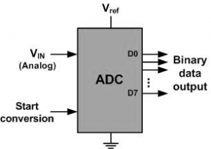
Therefore, we need an analog-to-digital (ADC) converter to translate the analog signals to digital numbers so that the micro controller can read and process the numbers.

Major characteristics of the ADC
Resolution
The ADC has n-bit resolution, where n can be 8, 10, 12, 16, or even 24 bits. Higher-resolution ADCs provide a smaller step size, where step size is the smallest change that can be discerned by an ADC. Some widely used resolutions for ADCs are shown in Table 11.1. Although the resolution of an ADC chip is decided at the time of its design and cannot be changed, we can control the step size with the help of what is called Vref.
| n-bit | Number of steps | Step size |
|---|---|---|
| 8 | 256 | 5V/256 = 19.53 mV |
| 10 | 1024 | 5V/1024 = 4.88 mV |
| 12 | 4096 | 5V/4096 = 1.2 mV |
| 16 | 65,536 | 5V/65,536 = 0.076 mV |
| Note: Vref = 5V | ||
Vref
Vref is an input voltage used for the reference voltage. The voltage connected to this pin, along with the resolution of the ADC chip, determine the step size. For an 8-bit ADC, the step size is Vref / 256 because it is an 8-bit ADC, and 2 to the power of 8 gives us 256 steps. See Table 11.1.
- If the analog input range needs to be 0 to 4 volts, Vref is connected to 4 volts. That gives 4 V / 256 = 15.62 mV for the step size of an 8-bit ADC.
- If we need a step size of 10 mV for an 8-bit ADC, then Vref = 2.56 V, because 2.56 V / 256 = 10 mV.
- For the 10-bit ADC, if the Vref = 5V, then the step size is 4.88 mV as shown in Table 11.1. Tables 11.2 and 11.3 show the relationship between the Vref and step size for the 8- and 10-bit ADCs, respectively.
- In some applications, we need the differential reference voltage where Vref = Vref (+) – Vref (–). Often the Vref (–) pin is connected to ground and the Vref (+) pin is used as the Vref.
| Vref (V) | Vin Range (V) | Step Size (mV) |
|---|---|---|
| 5.00 | 0 to 5 | 5 / 256 = 19.53 |
| 4.00 | 0 to 4 | 4 / 256 = 15.62 |
| 3.00 | 0 to 3 | 3 / 256 = 11.71 |
| 2.56 | 0 to 2.56 | 2.56 / 256 = 10 |
| 2.00 | 0 to 2 | 2 / 256 = 7.81 |
| 1.28 | 0 to 1.28 | 1.28 / 256 = 5 |
| 1.00 | 0 to 1 | 1 / 256 = 3.90 |
| Note: In an 8-bit ADC, step size is Vref/256 | ||
| Vref (V) | Vin Range (V) | Step Size (mV) |
|---|---|---|
| 5.00 | 0 to 5 | 5 / 1024 = 4.88 |
| 4.96 | 0 to 4.096 | 4.096 / 1024 = 4 |
| 3.00 | 0 to 3 | 3 / 1024 = 2.93 |
| 2.56 | 0 to 2.56 | 2.56 / 1024 = 2.5 |
| 2.00 | 0 to 2 | 2 / 1024 = 2 |
| 1.28 | 0 to 1.28 | 1.28 / 1024 = 1.25 |
| 1.024 | 0 to 1.024 | 1.024 / 1024 = 1 |
| Note: Vref Relation to Vin Range for an 10-bit ADC | ||
Conversion time
Conversion time is defined as the time it takes the ADC to convert the analog input to a digital number. The conversion time is dictated by the clock source connected to the ADC in addition to the method used for data conversion and technology used in the fabrication of the ADC.
Digital data output
In an 8-bit ADC we have an 8-bit digital data output of D0–D7, while in the 10-bit ADC the data output is D0–D9. To calculate the output voltage, we use the following formula:
DOUT = VIN / Step size
where Dout = digital data output (in decimal), Vin = analog input voltage, and step size (resolution) is the smallest change, which is Vref/256 for an 8-bit ADC.
Parallel versus Serial ADC
The ADC chips are either parallel or serial. In parallel ADC, we have 8 or more pins dedicated to bringing out the binary data, but in serial ADC we have only one pin for data out. The D0–D7 data pins of the 8-bit ADC provide an 8-bit parallel data path between the ADC chip and the CPU. In the case of the 16-bit parallel ADC chip, we need 16 pins for the data path.
In order to save pins, many 12- and 16-bit ADCs use pins D0–D7 to send out the upper and lower bytes of the binary data. In recent years, for many applications where space is a critical issue, using such a large number of pins for data is not feasible. For this reason, serial devices such as the serial ADC are becoming widely used. While the serial ADCs use fewer pins and their smaller packages take much less space on the printed circuit board, more CPU time is needed to get the converted data from the ADC because the CPU must get data one bit at a time, instead of in one single read operation as with the parallel ADC.
Analog input channels
Many data acquisition applications need more than one analog input for ADC. For this reason, we see ADC chips with 2, 4, 8, or even 16 channels on a single chip. Multiplexing of analog inputs is widely used allowing us to monitor multiple quantities such as temperature, pressure, flow, and so on. Nowadays, some ARM microcontroller chips come with 16-channel on-chip ADC.
Start conversion and end-of-conversion signals
For the conversion to be controlled by the CPU, there are needs for start conversion (SC) and end-of-conversion (EOC) signals. When SC is activated, the ADC starts converting the analog input value of Vin to a digital number. The amount of time it takes to convert varies depending on the conversion method. When the data conversion is complete, the end-of-conversion signal notifies the CPU that the converted data is ready to be picked up.
Recent Comments