
Interfacing to an LCD
LCD module pin descriptions
Hitachi HD44780 LCD controller dominated the character LCD modules. Most of the character LCD modules still use HD44780 or a variation of it. The HD44780 controller has a 14 pin interface for the microprocessor.
| Pin | Symbol | I/O | Description |
|---|---|---|---|
| 1 | VSS | — | Ground |
| 2 | VCC | — | +5v Power Supply |
| 3 | VEE | — | Power Supply to Control Contrast |
| 4 | RS | O | RS = 0 to Select Command Register, RS = 1 to Select Data Register |
| 5 | R/W | I/O | RW = 0 for Write RW = 1 for Read |
| 6 | E | O | Enable |
| 7 | DB0 | I/O | 8-bit data bus (DB0 – DB7) |
| 8 | DB1 | I/O | |
| 9 | DB2 | I/O | |
| 10 | DB3 | I/O | |
| 11 | DB4 | I/O | 4/8-bit data bus |
| 12 | DB5 | I/O | |
| 13 | DB6 | I/O | |
| 14 | DB7 | I/O | |
| 15 | LED+ | Supply Voltage for LED+ |
+5V |
| 16 | LED- | Supply Voltage for LED- |
0V |
VCC, VSS, and VEE: While VCC and VSS provide +5V power supply and ground, respectively, VEE is used for controlling the LCD contrast.
RS, register select: There are two registers inside the LCD and the RS pin is used for their selection as follows. If RS = 0, the instruction command code register is selected, allowing the user to send a command such as clear display, cursor at home, and so on (or query the busy status bit of the controller). If RS = 1, the data register is selected, allowing the user to send data to be displayed on the LCD (or to retrieve data from the LCD controller).
R/W, read/write: R/W input allows the user to write information into the LCD controller or read information from it. R/W = 1 when reading and R/W = 0 when writing.
E, enable: The enable pin is used by the LCD to latch information presented to its data pins. When data is supplied to data pins, a High-to-Low pulse must be applied to this pin in order for the LCD to latch in the data present at the data pins. This pulse must be a minimum of 230 ns wide, according to Hitachi datasheet.
D0 … D7: The 8-bit data pins are used to send information to the LCD or read the contents of the LCD’s internal registers. The LCD controller is capable of operating with 4-bit data and only D4-D7 are used.
There are four types of access cycles to the LCD controller depending on RS and R/W as shown in the following Table. Normally, you write ASCII characters into the data buffer (called DDRAM in the data sheets) to have them displayed on the screen. However, you can create up to 8 new characters by writing to the character generator RAM (CGRAM). These new characters exist as ASCII data 0 to 7.
| RS | R/W | Operation |
|---|---|---|
| 0 | 0 | Write a command to the LCD instruction register |
| 0 | 1 | Read Busy Flag (bit 7) |
| 1 | 0 | Write data to the LCD data buffer |
| 1 | 1 | Read data from the LCD to the microcontroller |
To display letters and numbers, we send ASCII codes for the letters A-Z, a-z, numbers 0-9, and the punctuation marks to these pins while making RS = 1.
There are also instruction command codes that can be sent to the LCD in order to clear the display, force the cursor to the home position, or blink the cursor. The following table lists some commonly used LCD Commands.
| Code (Hex) |
Command to LCD Instruction Register |
|---|---|
| 1 | clear Display Screen |
| 2 | Return Cursor Home |
| 6 | Increment Cursor (Shift Cursor to Right) |
| F | Display ON, Cursor Blinking |
| 80 | Force Cursor to beginning of 1st Line |
| C0 | Force Cursor to beginning of 2nd Line |
| 38 | 2 Lines and 5×7 character (8-bit data, D0 to D7) |
| 28 | 2 Lines and 5×7 character (4-bit data, D4 to D7) |
EduARM4 board LCD Connection
Jumper Selection:
J5 – Short 3 & 4
Sending commands to LCDs
To send any of the commands to the LCD, make pin RS = 0 and send a High-to-Low pulse on the E pin to enable the internal latch of the LCD.
Sending data to the LCD
In order to send data to the LCD to be displayed, we must set pin RS = 1, and also send a High-to-Low pulse to the E pin to enable the internal latch of the LCD.
LCD runs much slower than the micro controller. The first two commands in the above table take up to 1.64 ms to execute and all the other commands and data take up to 40 us. After one command or data is written to the LCD controller, one must wait until the LCD controller is ready before issuing the next command/data otherwise the second command/data will be ignored. An easy way is to delay the microcontroller for the maximam time it may take for the previous command.
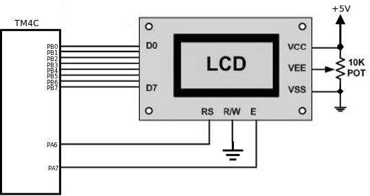
- The LCD’s data pins are connected to PORTB of the micro controller.
- The LCD’s RS pin is connected PORTA6 of the micro controller.
- The LCD’s R/W pin is connected to the ground (Always in write mode).
- The LCD’s E pin is connected to PORTA7 of the micro controller.
Both Ports x and y are configured as output ports.
Checking LCD busy flag
The above programs used a time delay before issuing the next data or command. This allows the LCD a sufficient amount of time to get ready to accept the next data. However, the LCD has a busy flag. We can monitor the busy flag and issue data when it is ready. This will speed up the process. To check the busy flag, we must read the command register (R/W = 1, RS = 0). The busy flag is the D7 bit of that register. Therefore, if R/W = 1, RS = 0; when D7 = 1 (busy flag = 1), the LCD is busy taking care of internal operations and will not accept any new information. When D7 = 0, the LCD is ready to receive new information.
Doing so requires switching the direction of the port connected to the data bus to input mode when polling the status register then switch the port direction back to output mode to send the next command. If the port direction is incorrect, it may damage the micro controller or the LCD module.
LCD Cursor Position
In the LCD, one can move the cursor to any location in the display by issuing an address command. The next character sent will appear at the cursor position. For the two-line LCD, the address command for the first location of line 1 is 0x80, and for line 2 it is 0xC0. The following table shows address locations and how they are accessed:
| RS | R/W | DB7 | DB6 | DB5 | DB4 | DB3 | DB2 | DB1 | DB0 |
|---|---|---|---|---|---|---|---|---|---|
| 0 | 0 | 1 | A6 | A5 | A4 | A3 | A2 | A1 | A0 |
where A6 A5 A4 A3 A2 A1 A0 = 0000000 to 0100111 for line 1 and A6 A5 A4 A3 A2 A1 A0 = 1000000 to 1100111 for line 2. See the following Table.
| DB7 | DB6 | DB5 | DB4 | DB3 | DB2 | DB1 | DB0 | |
|---|---|---|---|---|---|---|---|---|
| Line 1 (min) | 1 | 0 | 0 | 0 | 0 | 0 | 0 | 0 |
| Line 1 (max) | 1 | 0 | 1 | 0 | 0 | 1 | 1 | 1 |
| Line 2 (min) | 1 | 1 | 0 | 0 | 0 | 0 | 0 | 0 |
| Line 2 (max) | 1 | 1 | 1 | 0 | 0 | 1 | 1 | 1 |
The upper address range can go as high as 0100111 for the 40-character-wide LCD while for the 20-character-wide LCD the address of the visible positions goes up to 010011 (19 decimal = 10011 binary). Notice that the upper range 0100111 (binary) = 39 decimal, which corresponds to locations 0 to 39 for the LCDs of 40×2 size.
LCD Instructions
| Instruction | RS | R/W | DB7 | DB6 | DB5 | DB4 | DB3 | DB2 | DB1 | DB0 | Description | Execution Time(Max) |
|---|---|---|---|---|---|---|---|---|---|---|---|---|
| Clear Display |
0 | 0 | 0 | 0 | 0 | 0 | 0 | 0 | 0 | 1 | Clears entire display and sets DD RAM address 0 in address counter |
1.64 ms |
| Return Home |
0 | 0 | 0 | 0 | 0 | 0 | 0 | 0 | 1 | – | Sets DD RAM address to 0 as address counter. Also returns display being shifted to original positions. DD RAM contents remain unchanged. |
1.64 ms |
| Entry Mode Set |
0 | 0 | 0 | 0 | 0 | 0 | 0 | 1 | I/D | S | Sets cursor move direction and specifies shift of display. These operations are performed during data write and read. |
40us |
| Display On/Off Control |
0 | 0 | 0 | 0 | 0 | 0 | 1 | D | C | B | Sets On/Off of entire display (D), cursor On/Off (C), and blink of cursor position character (B) |
40us |
| Cursor or Display shift |
0 | 0 | 0 | 0 | 0 | 1 | S/C | R/L | – | – | Moves cursor and shifts display without changing DD RAM contents |
40us |
| Function Set |
0 | 0 | 0 | 0 | 1 | DL | N | F | – | – | Sets interface data length (DL), number of display lines (N), and character font (F) |
40us |
| Set CG RAM Address |
0 | 0 | 0 | 1 | AGC | Sets CG RAM address. CG RAM data is sent and received after this setting. |
40us | |||||
| Set DD RAM Address |
0 | 0 | 1 | ADD | Sets DD RAM address. DD RAM data is sent and received after this setting. |
40us | ||||||
| Read Busy Flag & Address |
0 | 1 | BF | AC | Reads Busy flag (BF) indicating internal operation is being performed and reads address counter contents. |
40us | ||||||
| Write Data CG or DD RAM |
1 | 0 | Write Data | Writes data into DD or CG RAM. |
40us | |||||||
| Read Data CG or DD RAM |
1 | 1 | Read Data | Reads data from DD or CG RAM. |
40us | |||||||
Abbreviations:
DD RAM: Display data RAM
CG RAM: Character generator RAM
AGC: CG RAM address
ADD: DD RAM address, corresponds to cursor address
AC: address counter used for both DD and CG RAM addresses
I/D: 1 = Increment, 0: Decrement
S =1: Accompanies display shift
S/C: 1 = Display shift, 0: Cursor move
R/L: 1: Shift to the right, 0: Shift to the left
DL: 1 = 8 bits, 0 = 4 bits
N: 1 = 2-line, 0 = 1-line
F: 1 = 5 x 10 dots, 0 = 5 x 7 dots
BF: 1 = Internal operation, 0 = Can accept instruction
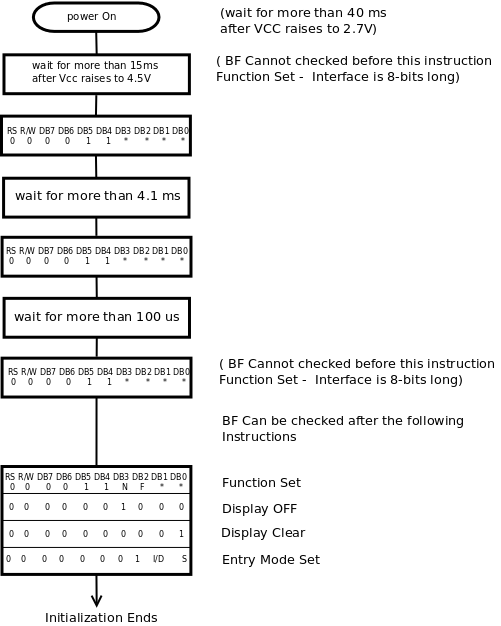
LCD Initialization (8-Bit Interface)
LCD Datasheet
See Also
Tasks
- Display “Welcome to DESE” on the 1st line and “Embedded Systems” on the 2nd line.
- The above text on both the lines should scroll from right to left at a reasonable rate.
- Create your own custom characters and Display it on 16×2 LCD screen.
Recent Comments