
Introduction:
A buck converter or step-down converter is a DC-to-DC converter which
decreases voltage, while increasing current, from its input (supply) to its output (load). It
is a class of switched-mode power supply. Switching converters (such as buck
converters) provide much greater power e iciency as DC-to-DC converters than linear
regulators, which are simpler circuits that dissipate power as heat, but do not step up
output current. The e iciency of buck converters can be very high, often over 90%,
making them useful for tasks such as converting a computer’s main supply voltage,
which is usually 12 V, down to lower voltages needed by USB, DRAM and the CPU, which
are usually 5, 3.3 or 1.8 V. It is a versatile power converter driving present day micro-
electronic and power level circuits.
Tiva launch pad TM1234C is a multi-purpose microcontroller board that is useful to
control some physical parameter in an Embedded system. It has various communication
modules like SPI,UART,I2C etc alongwith measurement and output blocks like ADC and
PWM. Schematic for this project is shown below:
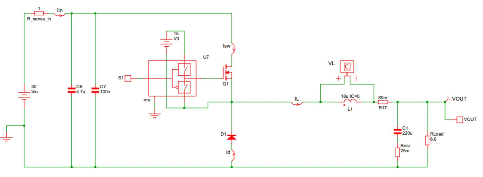
Fig 1- A simple Buck Converter
The idea is to read the output voltage using one of the two ADC modules of Tiva Board.
Each analog to digital converter uses same shared 12 analog input channels AN0-AN11.
The length of FIFO register is dependent on Sample sequencer (SS0 to SS3) being
selected. The resolution is 12 bit. This means the least count of measurement is:
Vmin=Vout/(2^12-1)
The plan is to use pin PE3 (port E of GPIO) for sensing the Vout and converting it to
digital value.The sampling frequency to be used is 250kHz. The complete closed loop
control with PWM block is shown below:
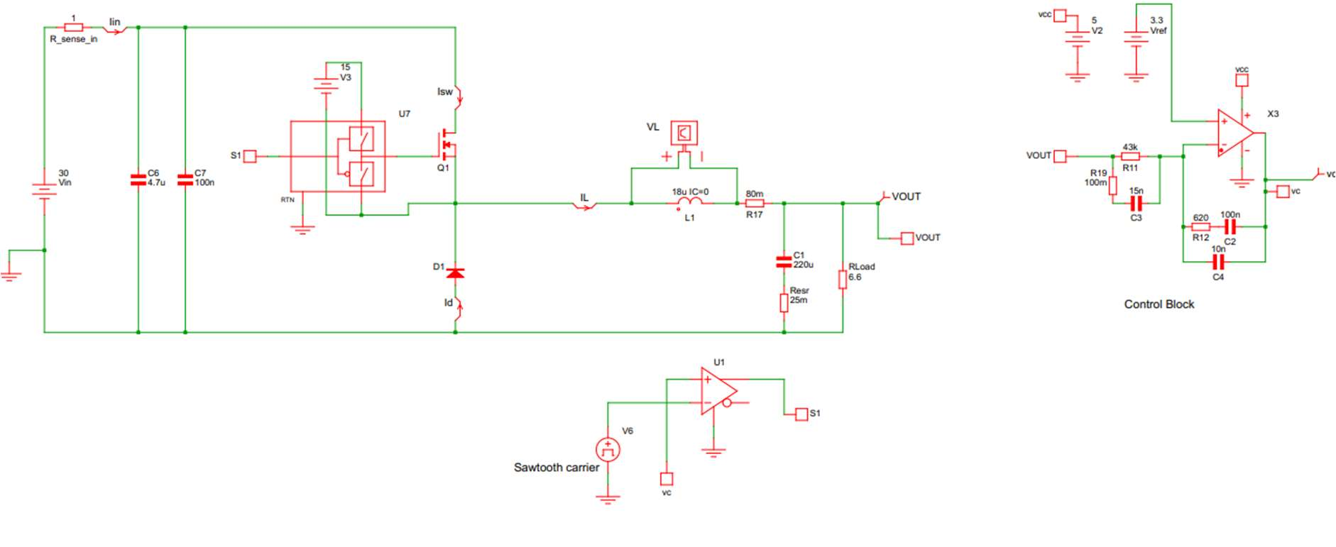
Fig 2- Control Block
Here, the Sallen-Key filter topology shown at right side is implemented through C-coding
in CCS in Tiva Board but the end-result remain same. Based on the sampled value of
output voltage and reference value of output voltage desired, a signal Vc shall be
generated that will act as input to the PWM Block.
The bottom part shown in fig 2 shows the PWM block where a sawtooth wave function is
compared with the Vc signal which was generated as output of ADC. The resulting output
of PWM block (with a gain of 1/Vm, where Vm=peak of sawtooth wave in Volts) is a pulse
width modulated signal that will drive the gate circuit of MOSFET and adjust the duty ratio
D.
D=Ton/Ts,
Ts=1/fs where fs is signal frequency of sawtooth carrier.
This PWM block implementation shall be done using one of the inbuilt PWM modules of
Tiva Board, whose output shall be fed to gate terminal of MOSFET. The model selected for
MOSFET is IRF840 which needs a 15 V gate drive. Thus the output of PWM needs
amplification from 5V to 15V for gate driving. It may be noted that the controller here is a
PI control which acts as low pass filter and only picks up low frequency change in the
Vout signal.
code:code_tiva
Video: A simple Buck Converter
Recent Comments